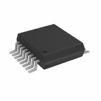
AD5934YRSZ Analog Devices Inc, AD5934YRSZ Datasheet - Page 24

AD5934YRSZ
Manufacturer Part Number
AD5934YRSZ
Description
IC NTWK ANALYZER 12B 1MSP 16SSOP
Manufacturer
Analog Devices Inc
Datasheet
1.AD5934YRSZ.pdf
(40 pages)
Specifications of AD5934YRSZ
Resolution (bits)
12 b
Master Fclk
16.776MHz
Voltage - Supply
2.7 V ~ 5.5 V
Operating Temperature
-40°C ~ 125°C
Mounting Type
Surface Mount
Package / Case
16-SSOP
Supply Voltage Range
2.7V To 5.5V
Operating Temperature Range
-40°C To +125°C
Digital Ic Case Style
SSOP
No. Of Pins
16
Frequency Max
0.1MHz
Termination Type
SMD
Filter Terminals
SMD
Rohs Compliant
Yes
Communication Function
Network Analyzer
Lead Free Status / RoHS Status
Lead free / RoHS Compliant
For Use With
EVAL-AD5934EBZ - BOARD EVALUATION FOR AD5934
Tuning Word Width (bits)
-
Lead Free Status / RoHS Status
Lead free / RoHS Compliant, Lead free / RoHS Compliant
Available stocks
Company
Part Number
Manufacturer
Quantity
Price
Company:
Part Number:
AD5934YRSZ
Manufacturer:
Analog Devices Inc
Quantity:
135
Company:
Part Number:
AD5934YRSZ
Manufacturer:
Maxim
Quantity:
289
Part Number:
AD5934YRSZ
Manufacturer:
ADI/亚德诺
Quantity:
20 000
Company:
Part Number:
AD5934YRSZ-REEL7
Manufacturer:
IR
Quantity:
114
AD5934
NUMBER OF INCREMENTS REGISTER (REGISTER
ADDRESS 0x88, REGISTER ADDRESS 0x89)
The default value of the number of increments register upon
reset is as follows: D8 to D0 are not reset at power-up. After a
reset command, the contents of this register are not reset.
Table 11. Number of Increments Register
Reg Addr
0x88
0x89
This register determines the number of frequency points in the
frequency sweep. The number of frequency points is represented
by a 9-bit word, D8 to D0. D15 to D9 are don’t care bits. This
register in conjunction with the start frequency register and the
frequency increment register determine the frequency sweep
range for the sweep operation. The maximum number of
increments that can be programmed is 511.
NUMBER OF SETTLING TIME CYCLES REGISTER
(REGISTER ADDRESS 0x8A, REGISTER ADDRESS
0x8B)
The default value of the number of settling time cycles register
upon reset is as follows: D10 to D0 are not reset at power-up.
After a reset command, the contents of this register are not reset.
This register determines the number of output excitation cycles
allowed to passthrough the unknown impedance after receipt of
a start frequency sweep, increment frequency, or repeat frequency
command, before the ADC is triggered to perform a conversion
of the response signal. The number of settling time cycles register
value determines the delay between a start frequency sweep/
increment frequency/repeat frequency command and the time
an ADC conversion commences. The number of cycles is
represented by a 9-bit word, D8 to D0. The value programmed
Table 13. Number of Settling Times Cycles Register
Register Address
0x8A
0x8B
Bits
D15 to D9
D8
D7 to D0
Bits
D15 to D11
D10 to D9
D8
D7 to D0
Description
Don’t care
Number of
increments
Number of
increments
Description
Don’t care
2-bit decode
D10
0
0
1
1
MSB number of settling time cycles
Number of settling time cycles
Function
Read or
write
Read or
write
Read or
write
D9
0
1
0
1
Format
Integer
number
stored
in binary
format
Integer
number
stored
in binary
format
Description
Default
No of cycles ×2
Reserved
No of cycles ×4
Rev. A | Page 24 of 40
into the number of settling time cycles register can be increased
by a factor of 2 or 4, depending on the status of Bits D10 to D9.
The five most significant bits, D15 to D11, are don’t care bits.
The maximum number of output cycles that can be programmed is
511 × 4 = 2044 cycles. For example, consider an excitation signal of
30 kHz, the maximum delay between the programming of this
frequency and the time that this signal is first sampled by the
ADC is ≈ 511 × 4 × 33.33 μs = 68.126 ms. The ADC takes 1024
samples, and the result is stored as real data and imaginary data in
Register Address 0x94 to Register Address 0x97. The conversion
process takes approximately 1 ms using a 16.777 MHz clock.
STATUS REGISTER (REGISTER ADDRESS 0x8F)
The status register is used to confirm that particular measurement
tests have been successfully completed. Each of the bits from D7 to
D0 indicate the status of a specific functionality of the AD5934.
Bit D0 and Bit D4 to Bit D7 are treated as don’t care bits; these
bits do not indicate the status of any measurement.
The status of Bit D1 indicates the status of a frequency point
impedance measurement. This bit is set when the AD5934
completes the current frequency point impedance measurement.
This bit indicates that there is valid real data and imaginary data
in Register Address 0x94 to Register Address 0x97. This bit is
reset on receipt of a start frequency sweep, increment frequency,
repeat frequency, or reset command. This bit is also reset at
power-up.
The status of Bit D2 indicates the status of the programmed
frequency sweep. This bit is set when all programmed increments
to the number of increments register are complete. This bit is
reset at power-up and on receipt of a reset command.
Table 12. Status Register 0x8F
Control Word
0000 0001
0000 0010
0000 0100
0000 1000
0001 0000
0010 0000
0100 0000
1000 0000
Function
Read or write
Read or write
Format
Integer number stored in binary format
Data
Description
Reserved
Valid real/imaginary data
Frequency sweep complete
Reserved
Reserved
Reserved
Reserved
Reserved


