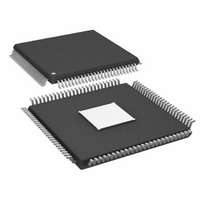
AD9910BSVZ Analog Devices Inc, AD9910BSVZ Datasheet - Page 17

AD9910BSVZ
Manufacturer Part Number
AD9910BSVZ
Description
IC DDS 1GSPS 14BIT PAR 100TQFP
Manufacturer
Analog Devices Inc
Datasheet
1.AD9910BSVZ-REEL.pdf
(64 pages)
Specifications of AD9910BSVZ
Design Resources
Synchronizing Multiple AD9910 1 GSPS Direct Digital Synthesizers (CN0121)
Resolution (bits)
14 b
Master Fclk
1GHz
Tuning Word Width (bits)
32 b
Voltage - Supply
1.8V, 3.3V
Operating Temperature
-40°C ~ 85°C
Mounting Type
Surface Mount
Package / Case
100-TQFP Exposed Pad, 100-eTQFP, 100-HTQFP, 100-VQFP
Pll Type
Frequency Synthesis
Frequency
1GHz
Supply Current
29mA
Supply Voltage Range
1.71V To 1.89V
Digital Ic Case Style
TQFP
No. Of Pins
100
Operating Temperature Range
-40°C To +85°C
Lead Free Status / RoHS Status
Lead free / RoHS Compliant
For Use With
AD9910/PCBZ - BOARD EVAL FOR AD9910 1GSPS
Lead Free Status / RoHS Status
Lead free / RoHS Compliant, Lead free / RoHS Compliant
Available stocks
Company
Part Number
Manufacturer
Quantity
Price
Company:
Part Number:
AD9910BSVZ
Manufacturer:
AVAGO
Quantity:
1 400
Company:
Part Number:
AD9910BSVZ
Manufacturer:
ADI
Quantity:
509
Company:
Part Number:
AD9910BSVZ
Manufacturer:
Analog Devices Inc
Quantity:
10 000
Part Number:
AD9910BSVZ
Manufacturer:
ADI/亚德诺
Quantity:
20 000
Company:
Part Number:
AD9910BSVZ-REEL
Manufacturer:
Analog Devices Inc
Quantity:
10 000
THEORY OF OPERATION
The AD9910 has four modes of operation.
•
•
•
•
The modes relate to the data source used to supply the DDS
with its signal control parameters: frequency, phase, or ampli-
tude. The partitioning of the data into different combinations
of frequency, phase, and amplitude is handled automatically
based on the mode and/or specific control bits.
In single tone mode, the DDS signal control parameters come
directly from the programming registers associated with the
serial I/O port. In RAM modulation mode, the DDS signal
control parameters are stored in the internal RAM and played
back upon command. In digital ramp modulation mode, the
DDS signal control parameters are delivered by a digital ramp
generator. In parallel data port modulation mode, the DDS
signal control parameters are driven directly into the parallel port.
The various modulation modes generally operate on only one of
the DDS signal control parameters (two in the case of the polar
modulation format). The unmodulated DDS signal control
parameters are stored in their appropriate programming
registers and automatically route to the DDS based on the
selected mode.
Single tone
RAM modulation
Digital ramp modulation
Parallel data port modulation
PROFILE[2:0]
I/O_UPDATE
TxENABLE
I/O_RESET
PARALLEL
DRHOLD
DROVER
PDCLK
DRCTL
INPUT
SCLK
SDIO
OSK
CS
16
2
2
2
3
PARALLEL DATA
TIMING AND
CONTROL
PROGRAMMING
REGISTERS
8
RAM_SWP_OVR
GENERATOR
DAC FSC
OUTPUT
KEYING
DIGITAL
SHIFT
RAMP
RAM
PARTITION
CONTROL
ROUTE
DATA
AND
Figure 22. Single Tone Mode
AMPLITUDE (A)
PHASE (θ)
FREQUENCY (ω)
Rev. C | Page 17 of 64
INTERNAL CLOCK TIMING
AND CONTROL
AD9910
CONTROL
POWER-
DOWN
CLOCK
A
ω
θ
DDS
A separate output shift keying (OSK) function is also available.
This function employs a separate digital linear ramp generator
that only affects the amplitude parameter of the DDS. The OSK
function has priority over the other data sources that can drive
the DDS amplitude parameter. As such, no other data source
can drive the DDS amplitude when the OSK function is enabled.
Although the various modes (including the OSK function) are
described independently, they can be enabled simultaneously.
This provides an unprecedented level of flexibility for generating
complex modulation schemes. However, to avoid multiple data
sources from driving the same DDS signal control parameter,
the device has a built-in priority protocol (see Table 5 in the
Mode Priority section).
SINGLE TONE MODE
In single tone mode, the DDS signal control parameters are
supplied directly from the programming registers. A profile is
an independent register that contains the DDS signal control
parameters. Eight profile registers are available.
Each profile is independently accessible. Use the three external
profile pins (PROFILE[2:0]) to select the desired profile. A
change in the state of the profile pins with the next rising edge
on SYNC_CLK updates the DDS with the parameters specified
by the selected profile.
Asin (ωt + θ)
Acos (ωt + θ)
SYNCHRONIZATION
MULTICHIP
SYSCLK
DAC FSC
2
2
INVERSE
FILTER
SINC
8
PLL
÷2
8-BIT
DAC
AUX
14-BIT
DAC
DAC_RSET
IOUT
IOUT
REFCLK_OUT
REF_CLK
REF_CLK
XTAL_SEL
AD9910


