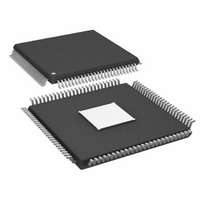
AD9910BSVZ Analog Devices Inc, AD9910BSVZ Datasheet - Page 25

AD9910BSVZ
Manufacturer Part Number
AD9910BSVZ
Description
IC DDS 1GSPS 14BIT PAR 100TQFP
Manufacturer
Analog Devices Inc
Datasheet
1.AD9910BSVZ-REEL.pdf
(64 pages)
Specifications of AD9910BSVZ
Design Resources
Synchronizing Multiple AD9910 1 GSPS Direct Digital Synthesizers (CN0121)
Resolution (bits)
14 b
Master Fclk
1GHz
Tuning Word Width (bits)
32 b
Voltage - Supply
1.8V, 3.3V
Operating Temperature
-40°C ~ 85°C
Mounting Type
Surface Mount
Package / Case
100-TQFP Exposed Pad, 100-eTQFP, 100-HTQFP, 100-VQFP
Pll Type
Frequency Synthesis
Frequency
1GHz
Supply Current
29mA
Supply Voltage Range
1.71V To 1.89V
Digital Ic Case Style
TQFP
No. Of Pins
100
Operating Temperature Range
-40°C To +85°C
Lead Free Status / RoHS Status
Lead free / RoHS Compliant
For Use With
AD9910/PCBZ - BOARD EVAL FOR AD9910 1GSPS
Lead Free Status / RoHS Status
Lead free / RoHS Compliant, Lead free / RoHS Compliant
Available stocks
Company
Part Number
Manufacturer
Quantity
Price
Company:
Part Number:
AD9910BSVZ
Manufacturer:
AVAGO
Quantity:
1 400
Company:
Part Number:
AD9910BSVZ
Manufacturer:
ADI
Quantity:
509
Company:
Part Number:
AD9910BSVZ
Manufacturer:
Analog Devices Inc
Quantity:
10 000
Part Number:
AD9910BSVZ
Manufacturer:
ADI/亚德诺
Quantity:
20 000
Company:
Part Number:
AD9910BSVZ-REEL
Manufacturer:
Analog Devices Inc
Quantity:
10 000
The PLL enable bit is used to choose between the PLL path or
the direct input path. When the direct input path is selected,
the REF_CLK/ REF_CLK pins must be driven by an external
signal source (single-ended or differential). Input frequencies
up to 2 GHz are supported. For input frequencies greater than
1 GHz, the input divider must be enabled for proper operation
of the device.
When the PLL is enabled, a buffered clock signal is available at
the REFCLK_OUT pin. This clock signal is the same frequency
as the REF_CLK input. This is especially useful when a crystal
is connected because it gives the user a replica of the crystal
clock for driving other external devices. The REFCLK_OUT has
programmable drive capability. This is controlled by two bits, as
listed in Table 7.
Table 7. REFCLK_OUT Buffer Control
DRV0 Bits (CFR3[29:28])
00
01
10
11
Crystal Driven REF_CLK/ REF_CLK
When using a crystal at the REF_CLK/ REF_CLK input, the
resonant frequency should be approximately 25 MHz.
shows the recommended circuit configuration. The internal
oscillator works with fundamental mode crystals only. Crystal
operation is enabled by a Logic 1 (1.8 V logic required) on the
XTAL_SEL pin.
REFCLK_OUT
REF_CLK
REF_CLK
94
90
91
REFCLK
INPUT DIVIDER
SELECT
LOGIC
INPUT
Figure 30. REF_CLK Block Diagram
[29:28]
DRV0
CFR3[14]
CFR3
REFCLK
RESETB
2
XTAL_SEL
÷2
1
0
95
1
0
REFCLK
INPUT DIVIDER BYPASS
CFR3[15]
[21:19]
CHARGE
ENABLE
IN
CFR3
2
PUMP
REFCLK_OUT Buffer
Disabled (tristate)
Low output current
Medium output current
High output current
I
CP
PLL_LOOP_FILTER
PLL_LOOP_FILTER
DIVIDE
CFR3
7
[7:1]
PLL
N
2
VCO SEL
SELECT
[26:24]
CFR3
3
VCO
OUT
PLL ENABLE
Figure 31
CFR3
[8]
1
0
SYSCLK
Rev. C | Page 25 of 64
Direct Driven REF_CLK/ REF_CLK
When driving the REF_CLK/ REF_CLK inputs directly from a
signal source, either single-ended or differential signals can be
used. With a differential signal source, the REF_CLK/ REF_CLK
pins are driven with complementary signals and ac-coupled with
0.1 μF capacitors. With a single-ended signal source, either a
single-ended-to-differential conversion can be employed or the
REF_CLK input can be driven single-ended directly. In either
case, 0.1 μF capacitors are used to ac couple both REF_CLK/
REF_CLK pins to avoid disturbing the internal dc bias voltage
of ~1.35 V. See
The REF_CLK/ REF_CLK input resistance is ~2.5 kΩ differential
(~1.2 kΩ single-ended). Most signal sources have relatively low
output impedances. The REF_CLK/ REF_CLK input resistance
is relatively high; therefore, its effect on the termination impedance
is negligible and can usually be chosen to be the same as the
output impedance of the signal source. The bottom two examples
in
Phase-Locked Loop (PLL) Multiplier
An internal phase-locked loop (PLL) provides the option to use
a reference clock frequency that is significantly lower than the
system clock frequency. The PLL supports a wide range of
programmable frequency multiplication factors (12× to 127×)
as well as a programmable charge pump current and external
SINGLE-ENDED SOURCE,
SINGLE-ENDED SOURCE,
Figure 32
DIFFERENTIAL SOURCE,
SINGLE-ENDED INPUT
DIFFERENTIAL INPUT
DIFFERENTIAL INPUT
assume a signal source with a 50 Ω output impedance.
Figure 32
Figure 31. Crystal Connection Diagram
Figure 32. Direct Connection Diagram
39pF
for more details.
LVPECL,
DRIVER
PECL,
LVDS
OR
39pF
XTAL
BALUN
50Ω
(1:1)
90
91
TERMINATION
REF_CLK
REF_CLK
50Ω
0.1µF
0.1µF
0.1µF
0.1µF
0.1µF
0.1µF
90
91
90
91
90
91
AD9910
REF_CLK
REF_CLK
REF_CLK
REF_CLK
REF_CLK
REF_CLK


