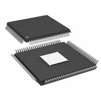
AD9910BSVZ Analog Devices Inc, AD9910BSVZ Datasheet - Page 23

AD9910BSVZ
Manufacturer Part Number
AD9910BSVZ
Description
IC DDS 1GSPS 14BIT PAR 100TQFP
Manufacturer
Analog Devices Inc
Datasheet
1.AD9910BSVZ-REEL.pdf
(64 pages)
Specifications of AD9910BSVZ
Design Resources
Synchronizing Multiple AD9910 1 GSPS Direct Digital Synthesizers (CN0121)
Resolution (bits)
14 b
Master Fclk
1GHz
Tuning Word Width (bits)
32 b
Voltage - Supply
1.8V, 3.3V
Operating Temperature
-40°C ~ 85°C
Mounting Type
Surface Mount
Package / Case
100-TQFP Exposed Pad, 100-eTQFP, 100-HTQFP, 100-VQFP
Pll Type
Frequency Synthesis
Frequency
1GHz
Supply Current
29mA
Supply Voltage Range
1.71V To 1.89V
Digital Ic Case Style
TQFP
No. Of Pins
100
Operating Temperature Range
-40°C To +85°C
Lead Free Status / RoHS Status
Lead free / RoHS Compliant
For Use With
AD9910/PCBZ - BOARD EVAL FOR AD9910 1GSPS
Lead Free Status / RoHS Status
Lead free / RoHS Compliant, Lead free / RoHS Compliant
Available stocks
Company
Part Number
Manufacturer
Quantity
Price
Company:
Part Number:
AD9910BSVZ
Manufacturer:
AVAGO
Quantity:
1 400
Company:
Part Number:
AD9910BSVZ
Manufacturer:
ADI
Quantity:
509
Company:
Part Number:
AD9910BSVZ
Manufacturer:
Analog Devices Inc
Quantity:
10 000
Part Number:
AD9910BSVZ
Manufacturer:
ADI/亚德诺
Quantity:
20 000
Company:
Part Number:
AD9910BSVZ-REEL
Manufacturer:
Analog Devices Inc
Quantity:
10 000
FUNCTIONAL BLOCK DETAIL
DDS CORE
The direct digital synthesizer (DDS) block generates a reference
signal (sine or cosine based on CFR1[16], the select DDS sine
output bit). The parameters of the reference signal (frequency,
phase, and amplitude) are applied to the DDS at its frequency,
phase offset, and amplitude control inputs, as shown in Figure 27.
The output frequency (f
frequency tuning word (FTW) at the frequency control input to
the DDS. The relationship among f
where FTW is a 32-bit integer ranging in value from 0 to
2,147,483,647 (2
full 32-bit range. This range constitutes frequencies from dc to
Nyquist (that is, ½ f
The FTW required to generate a desired value of f
by solving Equation 1 for FTW, as given in Equation 2.
where the round(x) function rounds the argument (the value of
x) to the nearest integer. This is required because the FTW is
constrained to be an integer value. For example, for f
41 MHz and f
(0x556AAAAB).
Programming an FTW greater than 2
image that appears at a frequency given by
The relative phase of the DDS signal can be digitally controlled
by means of a 16-bit phase offset word (POW). The phase offset
is applied prior to the angle-to-amplitude conversion block
internal to the DDS core. The relative phase offset (Δθ) is given by
FREQUENCY
AMPLITUDE
CONTROL
CONTROL
CONTROL
OFFSET
DDS SIGNAL CONTROL PARAMETERS
FTW
PHASE
f
f
OUT
OUT
=
=
=
32
⎛
⎜
⎝
⎛ −
⎜
⎝
14
16
round
1
SYSCLK
FTW
DDS_CLK
2
32
31
FTW
ACCUMULATOR
2
− 1), which represents the lower half of the
= 122.88 MHz, then FTW = 1,433,053,867
32
Figure 27. DDS Block Diagram
⎛
⎜
⎜
⎝
SYSCLK
⎞
⎟
⎠
32
32
2
32-BIT
f
SYSCLK
32
⎞
⎟
⎠
OUT
⎛
⎜
⎜
⎝
D Q
f
).
MSB ALIGNED
SYSCLK
R
ACCUMULATOR
RESET
f
SYSCLK
) of the AD9910 is controlled by the
f
OUT
32
19
OUT
⎞
⎟
⎟
⎠
⎞
⎟
⎟
⎠
(MSBs)
16
, FTW, and f
31
19
produces an aliased
CONVERSION
AMPLITUDE
ANGLE-TO-
(SINE OR
COSINE)
SYSCLK
(for FTW ≥ 2
OUT
OUT
is given by
is found
14
14
=
TO DAC
14
Rev. C | Page 23 of 64
(1)
(2)
31
)
where the upper quantity is for the phase offset expressed as
radian units and the lower quantity as degrees. To find the POW
value necessary to develop an arbitrary Δθ, solve the previous
equation for POW and round the result (in a manner similar
to that described previously for finding an arbitrary FTW).
The relative amplitude of the DDS signal can be digitally scaled
(relative to full scale) by means of a 14-bit amplitude scale
factor (ASF). The amplitude scale value is applied at the output
of the angle-to-amplitude conversion block internal to the DDS
core. The amplitude scale is given by
where the upper quantity is amplitude expressed as a fraction of
full scale and the lower quantity is expressed in decibels relative
to full scale. To find the ASF value necessary for a particular
scale factor, solve Equation 3 for ASF and round the result (in
a manner similar to that described previously for finding an
arbitrary FTW).
When the AD9910 is programmed to modulate any of the DDS
signal control parameters, the maximum modulation sample
rate is ¼ f
images at multiples of ¼ f
must be considered when using the device as a modulator.
14-BIT DAC OUTPUT
The AD9910 incorporates an integrated 14-bit, current output
DAC. The output current is delivered as a balanced signal using
two outputs. The use of balanced outputs reduces the potential
amount of common-mode noise present at the DAC output,
offering the advantage of an increased signal-to-noise ratio. An
external resistor (R
and AGND establishes the reference current. The full-scale
output current of the DAC (I
of the reference current (see the Auxiliary DAC section). The
recommended value of R
Attention should be paid to the load termination to keep the
output voltage within the specified compliance range; voltages
developed beyond this range cause excessive distortion and can
damage the DAC output circuitry.
Δ
Amplitude
θ
=
SYSCLK
2
360
π
⎛
⎜
⎝
⎛
⎜
⎝
. This means that the modulation signal exhibits
POW
POW
Scale
2
2
16
16
SET
⎞
⎟
⎠
) connected between the DAC_RSET pin
=
⎞
⎟
⎠
20
ASF
SET
2
SYSCLK
14
log
is 10 kΩ.
OUT
⎛
⎜
⎝
. The impact of these images
ASF
) is produced as a scaled version
2
14
⎞
⎟
⎠
AD9910
(3)


