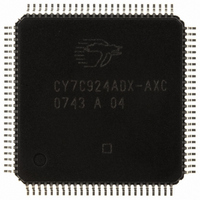
CY7C924ADX-AXC Cypress Semiconductor Corp, CY7C924ADX-AXC Datasheet - Page 26

CY7C924ADX-AXC
Manufacturer Part Number
CY7C924ADX-AXC
Description
IC TXRX HOTLINK 100LQFP
Manufacturer
Cypress Semiconductor Corp
Series
HOTlink™r
Type
Transceiverr
Specifications of CY7C924ADX-AXC
Package / Case
100-LQFP
Protocol
Fibre Channel
Voltage - Supply
4.5 V ~ 5.5 V
Mounting Type
Surface Mount
Product
Framer
Number Of Transceivers
1
Data Rate
622 Mbps
Supply Voltage (max)
5.5 V
Supply Voltage (min)
4.5 V
Supply Current (max)
250 mA
Maximum Operating Temperature
+ 70 C
Minimum Operating Temperature
0 C
Mounting Style
SMD/SMT
Operating Supply Voltage (typ)
5V
Screening Level
Commercial
Pin Count
100
Mounting
Surface Mount
Package Type
TQFP
Operating Supply Voltage (min)
4.5V
Operating Supply Voltage (max)
5.5V
Operating Temperature (min)
0C
Operating Temperature (max)
70C
Ic Interface Type
Parallel, Serial
Supply Voltage Range
4.5V To 5.5V
Operating Temperature Range
0°C To +70°C
Digital Ic Case Style
TQFP
No. Of Pins
100
No. Of Receivers
2
Frequency Max
50MHz
Rohs Compliant
Yes
Termination Type
SMD
Filter Terminals
SMD
Driver Case Style
TQFP
Lead Free Status / RoHS Status
Lead free / RoHS Compliant
Number Of Drivers/receivers
-
Lead Free Status / Rohs Status
Compliant
Other names
428-2918
CY7C924ADX-AXC
CY7C924ADX-AXC
Available stocks
Company
Part Number
Manufacturer
Quantity
Price
Company:
Part Number:
CY7C924ADX-AXC
Manufacturer:
CY
Quantity:
6
Company:
Part Number:
CY7C924ADX-AXC
Manufacturer:
CYPRESS
Quantity:
455
Company:
Part Number:
CY7C924ADX-AXC
Manufacturer:
Cypress Semiconductor Corp
Quantity:
10 000
Document #: 38-02008 Rev. *E
Maximum Ratings
(Above which the useful life may be impaired. For user guide-
lines, not tested.)
Storage Temperature ................................. –65°C to +150°C
Ambient Temperature with
Power Applied............................................. –55°C to +125°C
Supply Voltage to Ground Potential ............... –0.5V to +6.5V
DC Voltage Applied to Outputs
in High-Z State .......................................–0.5V to V
CY7C924ADX DC Electrical Characteristics
V
V
I
I
V
V
I
I
I
I
V
V
V
V
V
I
I
V
V
V
I
I
I
Notes
Parameter
OST
OZL
IHT
ILT
IHPD
ILPU
IHE
ILE
IHH
ILL
DD
4. Tested one output at a time, output shorted for less than one second, less than 10% duty cycle.
5. The output current and (resulting voltage swing) is set using a single resistor between CURSETx and V
6. To guarantee positive currents for all PECL voltages, an external pull-down resistor must be present.
7. Maximum I
TTL Outputs
TTL Inputs
Transmitter PECL-Compatible Output Pins: OUTA+, OUTA–, OUTB+, OUTB–
Receiver Single-ended PECL-compatible Input Pin: CARDET
Differential Line Receiver Input Pins: INA+, INA–, INB+, INB–
Miscellaneous
OHT
OLT
IHT
ILT
OHE
OLE
ODIF
IHE
ILE
DIFF
IHH
ILL
[6]
[7]
R
outputs unloaded.
CURSET
= (90*Z
Output HIGH Voltage
Output LOW Voltage
Output Short Circuit Current
High-Z Output Leakage Current
Input HIGH Voltage
Input LOW Voltage
Input HIGH Current
Input LOW Current
Input HIGH Current
Input LOW Current
Output HIGH Voltage (V
Output LOW Voltage (V
Output Differential Voltage
|(OUT+) – (OUT–)|
Input HIGH Voltage (V
Input LOW Voltage (V
Input HIGH Current
Input LOW Current
Input Differential Voltage |(IN+) – (IN–)|
Highest Input HIGH Voltage
Lowest Input LOW Voltage
Input HIGH Current
Input LOW Current
Power Supply Current
DD
is measured with V
LOAD
)/V
ODIF
, where Z
Description
DD
= MAX, RFEN = LOW, and outputs unloaded. Typical I
LOAD
DD
DD
DD
DD
referenced)
referenced)
is the differential load between the true and compliment outputs of the differential driver.
referenced)
referenced)
DD
+ 0.5V
I
I
V
V
V
V
V
Load = 50Ω to V
Load = 50Ω to V
Load = 50Ω to V
V
V
V
V
Freq. = Max.
OH
OL
Over the Operating Range
OUT
IN
IN
IN
IN
IN
IN
IN
IN
= 8 mA, V
= V
= 0.0V
= V
= 0.0V, Pins with internal pull-up
= V
= V
= V
= V
= –2 mA, V
= 0V
DD
DD
IHE
ILE
IHH
ILL
, Pins with internal pull-down
(min.)
(max.)
Min.
Output Current into TTL Outputs (LOW) ..................... 30 mA
DC Input Voltage ................................... –0.5V to V
Static Discharge Voltage.......................................... > 2001 V
(per MIL-STD-883, Method 3015)
Latch-up Current..................................................... > 200 mA
Operating Range
Max.
Commercial
Industrial
[4]
Test Conditions
DD
DD
Range
DD
DD
DD
= Min.
= Min.
– 1.33V R
– 1.33V R
– 1.33V R
DD
is measured with V
[5]
CURSET
CURSET
CURSET
SS
Ambient Temperature
. This CURSET resistor value is calculated as
–40°C to +85°C
0°C to +70°C
= 10k V
= 10k
= 10k
DD
= 5.0V, T
V
DD
DD
V
–300
–200
–0.5
Typ.
DD
Min
–30
–20
600
–40
200
170
2.4
2.0
2.5
2.5
– 1.165
A
– 1.03 V
CY7C924ADX
= 25°C, RFEN = LOW, and
– 2
V
V
DD
DD
DD
5.0V ± 10%
5.0V ± 10%
Page 26 of 58
+300
2500
Max.
1100
Max
–80
V
+40
–40
V
+40
V
750
250
0.4
0.8
– 1.475 V
20
– 1.62
– 0.83
DD
DD
DD
V
DD
DD
+ 0.5V
Unit
mA
mV
mV
mA
μA
μA
μA
μA
μA
μA
μA
μA
μA
V
V
V
V
V
V
V
V
V
[+] Feedback


