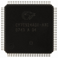
CY7C924ADX-AXC Cypress Semiconductor Corp, CY7C924ADX-AXC Datasheet - Page 4

CY7C924ADX-AXC
Manufacturer Part Number
CY7C924ADX-AXC
Description
IC TXRX HOTLINK 100LQFP
Manufacturer
Cypress Semiconductor Corp
Series
HOTlink™r
Type
Transceiverr
Specifications of CY7C924ADX-AXC
Package / Case
100-LQFP
Protocol
Fibre Channel
Voltage - Supply
4.5 V ~ 5.5 V
Mounting Type
Surface Mount
Product
Framer
Number Of Transceivers
1
Data Rate
622 Mbps
Supply Voltage (max)
5.5 V
Supply Voltage (min)
4.5 V
Supply Current (max)
250 mA
Maximum Operating Temperature
+ 70 C
Minimum Operating Temperature
0 C
Mounting Style
SMD/SMT
Operating Supply Voltage (typ)
5V
Screening Level
Commercial
Pin Count
100
Mounting
Surface Mount
Package Type
TQFP
Operating Supply Voltage (min)
4.5V
Operating Supply Voltage (max)
5.5V
Operating Temperature (min)
0C
Operating Temperature (max)
70C
Ic Interface Type
Parallel, Serial
Supply Voltage Range
4.5V To 5.5V
Operating Temperature Range
0°C To +70°C
Digital Ic Case Style
TQFP
No. Of Pins
100
No. Of Receivers
2
Frequency Max
50MHz
Rohs Compliant
Yes
Termination Type
SMD
Filter Terminals
SMD
Driver Case Style
TQFP
Lead Free Status / RoHS Status
Lead free / RoHS Compliant
Number Of Drivers/receivers
-
Lead Free Status / Rohs Status
Compliant
Other names
428-2918
CY7C924ADX-AXC
CY7C924ADX-AXC
Available stocks
Company
Part Number
Manufacturer
Quantity
Price
Company:
Part Number:
CY7C924ADX-AXC
Manufacturer:
CY
Quantity:
6
Company:
Part Number:
CY7C924ADX-AXC
Manufacturer:
CYPRESS
Quantity:
455
Company:
Part Number:
CY7C924ADX-AXC
Manufacturer:
Cypress Semiconductor Corp
Quantity:
10 000
Document #: 38-02008 Rev. *E
Pin Descriptions
CY7C924ADX HOTLink Transceiver
44, 42,
40, 36,
34, 32,
30, 22
46
54
56
58
Number
Transmit Path Signals
Pin
TXDATA[7:0]
TXINT/
TXDATA[8]
TXHALT*/
TXDATA[9]
TXSVS/
TXDATA[10]
TXSOC/
TXDATA[11]
Name
TTL input, sampled
on TXCLK↑ or
REFCLK↑,
Internal Pull Up
TTL input, sampled
on TXCLK↑ or
REFCLK↑,
Internal Pull Up
TTL input, sampled
on TXCLK↑ or
REFCLK↑,
Internal Pull Up
TTL input, sampled
on TXCLK↑ or
REFCLK↑,
Internal Pull Up
TTL input, sampled
on TXCLK↑ or
REFCLK↑,
Internal Pull Up
I/O Characteristics
Parallel Transmit Data Input. Bus width can be configured to accept either
8 or 10 bit characters. When the encoder is bypassed (ENCBYP* is LOW),
TXDATA[7:0] functions as the least significant eight bits of the 10 or 12 bit
preencoded transmit character.
Transmit Interrupt Input. This input is only interpreted if both the Transmit
FIFO and encoder are enabled (FIFOBYP* and ENCBYP* are HIGH). Any
state change (0→1 or 1→0) in TXINT, forces a character into the transmit
encoder and shifter before accessing the next Transmit FIFO contents. This
signal passes around, not through, the Transmit FIFO.
When TXINT transitions from 0→1, a C0.0 (K28.0) special code is sent. When
TXINT transitions from 1→0, a C3.0 (K28.3) special code is sent. These
special codes force a similar signal transition on the RXINT output of an
attached CY7C924ADX HOTLink Transceiver.
When the Transmit FIFO is bypassed and the encoder is enabled (FIFOBYP*
is LOW and ENCBYP* is HIGH), this input is ignored.
When the Transmit FIFO is bypassed and the encoder is bypassed
(FIFOBYP* and ENCBYP* are LOW), TXDATA[8] functions as the 9th bit of
the 10 or 12 bit preencoded transmit character.
Transmit FIFO Halt Immediate Input. When the Transmit FIFO and the
encoder are enabled (FIFOBYP* and ENCBYP* are HIGH) and TXHALT*
asserts LOW, data transmission from the FIFO is suspended and the HOTLink
transmits idle characters (K28.5). During this time, data can still be loaded into
the FIFO. When TXHALT* is deasserted HIGH, normal data processing
proceeds.
When the encoder is bypassed (ENCBYP* is LOW), TXDATA[9] always
functions as the tenth bit of the 10 or 12 bit preencoded transmit character.
When the Transmit FIFO is bypassed and the encoder is enabled (FIFOBYP*
is LOW and ENCBYP* is HIGH), this input is ignored
Transmit Send Violation Symbol Input. When the encoder is enabled and
the Transmit FIFO is enabled (ENCBYP* and FIFOBYP* are HIGH), this input
is interpreted along with TXSOC and TXSC/D* (see
details). When the Transmit FIFO is disabled (FIFOBYP* is LOW) and the
TXSVS bit is set, the character on the TXDATA is ignored and a C0.7 exception
is sent instead.
When the encoder is bypassed and in 10 bit mode (ENCBYP* and BYTE8/10*
are LOW), TXDATA[10] functions as the eleventh bit of the 12 bit preencoded
transmit character.
When the Encoder is bypassed and in 8 bit mode (ENCBYP* is LOW and
BYTE8/10* is HIGH), this input is ignored.
Transmit Start of Cell Input. When the Transmit FIFO and encoder are
enabled (ENCBYP* and FIFOBYP* are HIGH), this input is a message frame
delimiter that indicates the beginning of a data packet. It is interpreted along
with TXSVS and TXSC/D* (see
When the Transmit FIFO is bypassed (FIFOBYP* is LOW) and the encoder is
enabled (ENCBYP* is HIGH) this input is ignored.
When in 12 bit encoder bypass mode (ENCBYP* and BYTE8/10* are LOW),
TXDATA[11] functions as the twelfth bit (MSB) of the 12 bit preencoded
transmit character.
When the encoder is bypassed and in 8 bit mode (ENCBYP* is LOW and
BYTE8/10* is HIGH), this input is ignored.
Signal Description
Table 2
for details).
Table 2 on page 15
CY7C924ADX
Page 4 of 58
for
[+] Feedback


