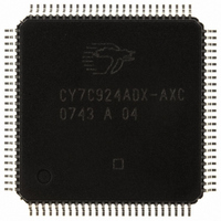
CY7C924ADX-AXC Cypress Semiconductor Corp, CY7C924ADX-AXC Datasheet - Page 6

CY7C924ADX-AXC
Manufacturer Part Number
CY7C924ADX-AXC
Description
IC TXRX HOTLINK 100LQFP
Manufacturer
Cypress Semiconductor Corp
Series
HOTlink™r
Type
Transceiverr
Specifications of CY7C924ADX-AXC
Package / Case
100-LQFP
Protocol
Fibre Channel
Voltage - Supply
4.5 V ~ 5.5 V
Mounting Type
Surface Mount
Product
Framer
Number Of Transceivers
1
Data Rate
622 Mbps
Supply Voltage (max)
5.5 V
Supply Voltage (min)
4.5 V
Supply Current (max)
250 mA
Maximum Operating Temperature
+ 70 C
Minimum Operating Temperature
0 C
Mounting Style
SMD/SMT
Operating Supply Voltage (typ)
5V
Screening Level
Commercial
Pin Count
100
Mounting
Surface Mount
Package Type
TQFP
Operating Supply Voltage (min)
4.5V
Operating Supply Voltage (max)
5.5V
Operating Temperature (min)
0C
Operating Temperature (max)
70C
Ic Interface Type
Parallel, Serial
Supply Voltage Range
4.5V To 5.5V
Operating Temperature Range
0°C To +70°C
Digital Ic Case Style
TQFP
No. Of Pins
100
No. Of Receivers
2
Frequency Max
50MHz
Rohs Compliant
Yes
Termination Type
SMD
Filter Terminals
SMD
Driver Case Style
TQFP
Lead Free Status / RoHS Status
Lead free / RoHS Compliant
Number Of Drivers/receivers
-
Lead Free Status / Rohs Status
Compliant
Other names
428-2918
CY7C924ADX-AXC
CY7C924ADX-AXC
Available stocks
Company
Part Number
Manufacturer
Quantity
Price
Company:
Part Number:
CY7C924ADX-AXC
Manufacturer:
CY
Quantity:
6
Company:
Part Number:
CY7C924ADX-AXC
Manufacturer:
CYPRESS
Quantity:
455
Company:
Part Number:
CY7C924ADX-AXC
Manufacturer:
Cypress Semiconductor Corp
Quantity:
10 000
Document #: 38-02008 Rev. *E
Pin Descriptions
CY7C924ADX HOTLink Transceiver
70
60
16
7
41, 43,
45, 47,
48, 53,
59, 61
33
Number
Receive Path Signals
Pin
TXHALF*
TXEMPTY*
TXRST*
TXBISTEN*
RXDATA[7:0]
RXINT/
RXDATA[8]
Name
(continued)
3-state TTL output,
changes following
TXCLK↑ or
REFCLK↑
3-state TTL output,
changes following
TXCLK↑ or
REFCLK↑
TTL input, internal
pull-up, sampled on
TXCLK↑,
Internal Pull Up
TTL input,
asynchronous,
Internal Pull Up
Bidirectional TTL,
changes following
RXCLK↑, or sampled
by RXCLK↑
Bidirectional TTL,
changes following
RXCLK↑, or sampled
by RXCLK↑
I/O Characteristics
Transmit FIFO Half-full Status Flag. The TXHALF* flag is always active
LOW, regardless of the EXTFIFO* setting.
When the Transmit FIFO is enabled, TXHALF* is asserted LOW when the
Transmit FIFO is half full or more (128 characters).
TXHALF* is only set to High-Z state by the assertion of RESET*[1:0] LOW.
Transmit FIFO Empty Status Flag. Active HIGH when configured for
Cascade timing (EXTFIFO is HIGH), active LOW when configured for UTOPIA
timing (EXTFIFO is LOW). The TXEMPTY* output is enabled when AM* is
asserted, otherwise it is High-Z
When the Transmit FIFO is enabled (FIFOBYP* is HIGH), TXEMPTY* is
asserted either when no data has been loaded into the Transmit FIFO, or when
the Transmit FIFO has been emptied by either a Transmit FIFO reset or by
the normal transmission of the FIFO contents.
When the Transmit FIFO is bypassed (FIFOBYP* is LOW), TXEMPTY* is
asserted to indicate that the transmitter can accept data.
When TXBISTEN* is asserted LOW, TXEMPTY* becomes the transmit
BIST-progress indicator (regardless of the logic state of FIFOBYP*). In this
mode TXEMPTY* is asserted for one TXCLK or REFCLK period at the end of
each transmitted BIST sequence, depending on the FIFOBYP* setting.
Transmit FIFO Reset. When TXRST* is asserted for eight or more TXCLK
cycles, a reset operation begins on the Transmit FIFO. This input is ignored
when the Transmit FIFO is bypassed.
Transmitter BIST Enable. When TXBISTEN* is LOW, the transmitter
generates a 511-character repeating built-in self test (BIST) sequence, that
can validate link integrity. The transmitter returns to normal operation when
TXBISTEN* is HIGH. All Transmit FIFO read operations suspend when BIST
is active.
Parallel Data Output and Serial Address Register Access. These outputs
change following the rising edge of RXCLK, when enabled to output data (the
device is addressed by AM* and selected by RXEN*). The contents of this bus
are interpreted differently based on the levels present on ENCBYP*,
BYTE8/10*, RXSC/D*, and when accessing the Serial Address Register.
When the decoder is bypassed (ENCBYP* is LOW), RXDATA[7:0] functions
as the least significant eight bits of the 10 or 12 bit preencoded receive
character.
Receive Interrupt Output. When the Receive FIFO and decoder are enabled
(FIFOBYP* and ENCBYP* are HIGH) and a C0.0 (K28.0) special code is
received, RXINT is set HIGH. When a C3.0 (K28.3) special code is received
RXINT is set LOW. These special codes are generated in response to equiv-
alent transitions on the TXINT input of an attached CY7C924ADX HOTLink
transceiver.
This signal is extracted before the Receive FIFO and (except for Receive
Discard Policy 0) the associated command codes are not considered “data”
to be entered into the Receive FIFO and are discarded.
When the Receive FIFO is bypassed (FIFOBYP* is LOW) and the decoder is
enabled (ENCBYP* is HIGH), this output has no function.
When the decoder is bypassed (ENCBYP* is LOW), RXDATA[8] functions as
the ninth bit of the 10 or 12 bit undecoded receive character.
Signal Description
CY7C924ADX
Page 6 of 58
[+] Feedback


