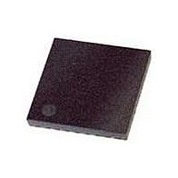
ispPAC-POWR607-01N32I Lattice, ispPAC-POWR607-01N32I Datasheet - Page 3

ispPAC-POWR607-01N32I
Manufacturer Part Number
ispPAC-POWR607-01N32I
Description
Supervisory Circuits Prec. Prog. Pwr Sppl y Seq. Mon. I
Manufacturer
Lattice
Datasheet
1.PAC-POWR607-EV.pdf
(28 pages)
Specifications of ispPAC-POWR607-01N32I
Number Of Voltages Monitored
6
Undervoltage Threshold
0.8 V
Output Type
Open Collector / Drain
Manual Reset
Resettable
Watchdog
Watchdog
Power-up Reset Delay (typ)
300 us
Supply Voltage (max)
3.96 V
Supply Voltage (min)
2.64 V
Supply Current (typ)
3.5 mA
Mounting Style
SMD/SMT
Package / Case
QFN-32
Lead Free Status / Rohs Status
Lead free / RoHS Compliant
Pin Descriptions (Cont.)
Lattice Semiconductor
1. GND pins must be connected together on the circuit board.
2. Open-drain outputs require an external pull-up resistor to a supply.
3. IN1_PWRDN and IN2 are inputs to the PLD. The thresholds for these pins are referenced by the voltage on VCC.
4. The power-down function is E
5. Source of the power-down initiation can be assigned to either the IN1_PWRDN pin or to an internally generated PLD output signal called
6. VCC pins must be connected together on the circuit board.
7. In power-down mode, VCCJ is internally pulled to GND to turn off the JTAG I/O pins. It is important, therefore, that the VCCJ pin be open
8. The VMON inputs can be biased independently from VCC. Unused VMON inputs should be tied to GND.
9. Thresholds of IN_OUT3...IN_OUT7 in the input mode are referenced by the voltage on VCC.
1, 8, 9, 16, 17,
down mode = high).
PLD_PWRDN. When generated internally by the PLD, the IN1_PWRDN pin is only used to exit power-down mode (IN1_PWRDN pin =
high).
whenever power-down mode is initiated. If connected to a power supply during power-down mode, VCCJ will draw approximately 2.2mA.
24, 25, 32
Number
Die Pad
4, 21
28
15
18
14
19
13
10
2
3
5
6
7
VMON1
VMON2
VMON3
VMON4
VMON5
VMON6
Name
VCCJ
TDO
TMS
VCC
TCK
TDI
IN2
NC
NC
2
CMOS programmable and when enabled is input level sensitive (enter power-down mode = low; exit power-
Digital Input
Digital Input
Digital Input
Digital Output
Digital Input
Power
Power
Analog Input
Analog Input
Analog Input
Analog Input
Analog Input
Analog Input
No Connection
No Connection
Pin Type
0V to 5.5V
0V to 5.5V
0V to 5.5V
0V to 5.5V
0V to 5.5V
2.64V to 3.96V
2.25V to 3.6V
-0.3V to 5.9V
-0.3V to 5.9V
-0.3V to 5.9V
-0.3V to 5.9V
-0.3V to 5.9V
-0.3V to 5.9V
Not applicable
Not applicable
4-3
Voltage Range
3
8
8
8
8
8
8
PLD Logic Input 2. When not used, this pin
should be tied to GND.
JTAG Test Clock Input
JTAG Test Data In - Internal Pull-up
JTAG Test Data Out
JTAG Test Mode Select - Internal Pull-up
Power Supply
VCC for JTAG Logic Interface Pins
Voltage Monitor Input 1
Voltage Monitor Input 2
Voltage Monitor Input 3
Voltage Monitor Input 4
Voltage Monitor Input 5
Voltage Monitor Input 6
No internal connection
No internal connection
ispPAC-POWR607 Data Sheet
6
Description
7


