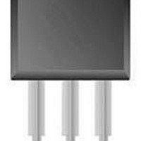
BUK9520-55 NXP Semiconductors, BUK9520-55 Datasheet

BUK9520-55
Manufacturer Part Number
BUK9520-55
Description
MOSFET Power RAIL PWR-MOS
Manufacturer
NXP Semiconductors
Specifications of BUK9520-55
Configuration
Single
Transistor Polarity
N-Channel
Resistance Drain-source Rds (on)
0.02 Ohms
Drain-source Breakdown Voltage
55 V
Gate-source Breakdown Voltage
+/- 10 V
Continuous Drain Current
52 A
Power Dissipation
116 W
Maximum Operating Temperature
+ 175 C
Mounting Style
Through Hole
Package / Case
TO-220AB
Minimum Operating Temperature
- 55 C
Lead Free Status / Rohs Status
Details
Other names
BUK9520-55,127
Available stocks
Company
Part Number
Manufacturer
Quantity
Price
Company:
Part Number:
BUK9520-55
Manufacturer:
PHILIPS
Quantity:
5 000
Company:
Part Number:
BUK9520-55
Manufacturer:
NXP
Quantity:
12 500
Part Number:
BUK9520-55
Manufacturer:
PHILIPS/飞利浦
Quantity:
20 000
Company:
Part Number:
BUK9520-55A
Manufacturer:
NXP
Quantity:
36 000
Company:
Part Number:
BUK9520-55A
Manufacturer:
NXP
Quantity:
12 500
Philips Semiconductors
GENERAL DESCRIPTION
N-channel enhancement mode logic
level field-effect power transistor in a
plastic
technology. The device features very
low on-state resistance and has
integral zener diodes giving ESD
protection up to 2kV. It is intended for
use in automotive and general
purpose switching applications.
PINNING - TO220AB
LIMITING VALUES
Limiting values in accordance with the Absolute Maximum System (IEC 134)
ESD LIMITING VALUE
THERMAL RESISTANCES
April 1998
TrenchMOS
Logic level FET
SYMBOL
V
V
I
I
I
P
T
SYMBOL
V
SYMBOL
R
R
D
D
DM
PIN
V
stg
DS
DGR
tot
C
tab
th j-mb
th j-a
1
2
3
GS
, T
j
envelope
gate
drain
source
drain
DESCRIPTION
PARAMETER
Drain-source voltage
Drain-gate voltage
Gate-source voltage
Drain current (DC)
Drain current (DC)
Drain current (pulse peak value)
Total power dissipation
Storage & operating temperature
PARAMETER
Electrostatic discharge capacitor
voltage, all pins
PARAMETER
Thermal resistance junction to
mounting base
Thermal resistance junction to
ambient
using
transistor
’trench’
QUICK REFERENCE DATA
PIN CONFIGURATION
SYMBOL
V
I
P
T
R
D
j
DS
tot
DS(ON)
CONDITIONS
-
R
-
T
T
T
T
-
CONDITIONS
Human body model
(100 pF, 1.5 k )
CONDITIONS
-
in free air
mb
mb
mb
mb
GS
tab
PARAMETER
Drain-source voltage
Drain current (DC)
Total power dissipation
Junction temperature
Drain-source on-state
resistance
= 25 ˚C
= 100 ˚C
= 25 ˚C
= 25 ˚C
= 20 k
1 2 3
1
V
GS
= 5 V
SYMBOL
TYP.
MIN.
MIN.
- 55
60
-
-
-
-
-
-
-
-
-
g
MAX.
Product specification
116
175
55
52
20
MAX.
MAX.
MAX.
1.29
208
116
175
55
55
10
52
37
2
BUK9520-55
-
d
s
Rev 1.100
UNIT
UNIT
UNIT
K/W
K/W
UNIT
kV
W
˚C
m
V
V
V
A
A
A
W
˚C
V
A


