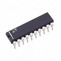
LTC1061CN Linear Technology, LTC1061CN Datasheet - Page 10

LTC1061CN
Manufacturer Part Number
LTC1061CN
Description
IC FILTER BUILDNG BLK TRPL 20DIP
Manufacturer
Linear Technology
Datasheet
1.LTC1061CNPBF.pdf
(16 pages)
Specifications of LTC1061CN
Filter Type
Universal Switched Capacitor
Frequency - Cutoff Or Center
35kHz
Number Of Filters
3
Max-order
6th
Voltage - Supply
4.74 V ~ 16 V, ±2.37 V ~ 8 V
Mounting Type
Through Hole
Package / Case
20-DIP (0.300", 7.62mm)
Lead Free Status / RoHS Status
Contains lead / RoHS non-compliant
Available stocks
Company
Part Number
Manufacturer
Quantity
Price
Company:
Part Number:
LTC1061CN
Manufacturer:
LT
Quantity:
5 510
Company:
Part Number:
LTC1061CN
Manufacturer:
TI
Quantity:
5 510
Company:
Part Number:
LTC1061CN#PBF
Manufacturer:
LT
Quantity:
872
W
LTC1061
Figure 13 shows the measured frequency response of the
circuit Figure 12 configured to provide a notch function.
The filter output is taken out of pin 3. The resistor values
are standard 1%.
The ratio of the 0dB width, BW1, to the notch width BW2,
is 5:1 and matches the theoretical design value. The
measured notch depth was –53dB versus –56dB theoreti-
cal and the clock-to-center notch frequency ratio is 100:1.
Figure 14 shows the measured frequency response of the
circuit topology, Figure 12, but with pole/zero locations
configured to provide a high Q, 6th order elliptic bandpass
filter operating with a clock-to-center frequency ratio of
50:1 or 100:1. The theoretical passband ripple, stopband
attenuation and stopband to ripple bandwidth ratio are
0.5dB, 56dB, 5:1 respectively. The obtained results with
1% standard resistor values closely match the theoretical
frequency response. For this application, the normalized
10
CLOCK INPUT
ODES OF OPERATIO
T
2
L, CMOS
Figure 12. 6th Order Elliptic Bandpass, Lowpass
or Notch Topology
V
V
IN
+
NOTES: FOR NOTCH RESPONSES, PIN 7 SHOULD BE
PREFERABLY CONNECTED TO GROUND AND THE
FILTER OUTPUT IS PIN 3.
FOR BANDPASS OR LOWPASS RESPONSES, PIN 7
CAN BE EITHER AT GROUND OR POSITIVE SUPPLY,
AND THE FILTER OUTPUT IS PIN 2 OR PIN 1.
R23
R33
10
1
2
3
4
5
6
7
8
9
LTC1061
20
19
18
17
16
15
14
13
12
11
R
l
2
U
V
R
R32
R22
–
R42
h
2
R
R41
l
R31
R21
R
R11
1
h
1
1061 F12
center frequencies, Qs, and notch frequencies are (f
0.969, Q1 = 54.3, f
1.187, f
output of Side A, Pin 2.
Lowpass filters with stopband notches can also be realized
by using Figure 12 provided that 6th order lowpass filter
approximations with 2 stopband notches can be synthe-
sized. Literature describing elliptic double terminated (RLC)
Figure 14. Resistor Values and Amplitude Response of Figure 12
Topology. The Bandpass Filter is Centered Around 2600Hz when
Operating with a 130kHz Clock.
–10
–30
–40
–50
–60
–70
–10
–30
–40
–50
–60
–70
–80
–90
–20
–20
Figure 13. Resistor Values and Amplitude Response of
Figure 12 Topology. The Notch is Centered at 2600Hz.
0
0
1.0
1.0
V
f
CLK
V
f
S
CLK
O3
S
= ±5V
= ±5V
= 260kHz
1.5
= 130kHz
1.5
= 1, Q3 = 26.2). The output of the filter is the BP
2.0
2.0
f
f
BW2
IN
IN
n1
(kHz)
(kHz)
= 0.84, f
2.5
2.5
2.6kHz
BW1
3.0
3.0
O2
= 1.031, Q2 = 54.3, f
3.5
3.5
R11 = 165k
R31 = 143k
R
R22 = 20k
R42 = 15.4k
R
R33 = 169k
NOTES: USE A 15pF CAPACITOR
BETWEEN PINS 17 AND 18.
PIN 7 IS GROUNDED.
NOTE: FOR CLOCK FREQUENCIES
ABOVE 500kHz, CONNECT A 5pF
IN PARALLEL WITH R41 AND R42.
R11 = 576k
R31 = 562k
R
R22 = 10.7k
R42 = 10k
R
R33 = 75k
h
l
h
l
2 = 10k
2 = 10k
1 = 10k
11 = 28.7k
RESISTOR VALUES
RESISTOR VALUES
STANDARD 1%
STANDARD 1%
R21 = 10k
R41 = 13k
R
R32 = 221k
R
R23 = 84.5k
R21 = 10k
R41 = 10.7k
R
R32 = 562k
R
R23 = 2.94k
l
h
1 = 10.5k
l
h
2 = 10.5k
11 = 40.2k
2 = 14k
1061 F13
1061 F14
O1
1061fe
n2
=
=


