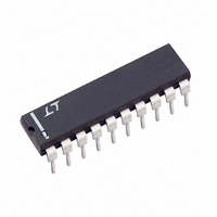
LTC1061CN Linear Technology, LTC1061CN Datasheet - Page 8

LTC1061CN
Manufacturer Part Number
LTC1061CN
Description
IC FILTER BUILDNG BLK TRPL 20DIP
Manufacturer
Linear Technology
Datasheet
1.LTC1061CNPBF.pdf
(16 pages)
Specifications of LTC1061CN
Filter Type
Universal Switched Capacitor
Frequency - Cutoff Or Center
35kHz
Number Of Filters
3
Max-order
6th
Voltage - Supply
4.74 V ~ 16 V, ±2.37 V ~ 8 V
Mounting Type
Through Hole
Package / Case
20-DIP (0.300", 7.62mm)
Lead Free Status / RoHS Status
Contains lead / RoHS non-compliant
Available stocks
Company
Part Number
Manufacturer
Quantity
Price
Company:
Part Number:
LTC1061CN
Manufacturer:
LT
Quantity:
5 510
Company:
Part Number:
LTC1061CN
Manufacturer:
TI
Quantity:
5 510
Company:
Part Number:
LTC1061CN#PBF
Manufacturer:
LT
Quantity:
872
W
LTC1061
2. Secondary Modes: Mode 1b – It is derived from Mode
1. In Mode 1b, Figure 7, two additional resistors, R5 and
R6, are added to attenuate the amount of voltage fed back
from the lowpass output into the input of the S
switched capacitor summer. This allows the filter clock-
to-center frequency ratio to be adjusted beyond 50:1 (or
100:1). Mode 1b still maintains the speed advantages of
Mode 1. Figure 8 shows the 3 lowpass sections of the
LTC1061 in cascade resulting in a Chebyshev lowpass
filter. The side A of the IC is connected in Mode 1b to
provide the first resonant frequency below the cutoff
frequency of the filter. The practical ripple, obtained by
using a non-A version of the LTC1061 and 1% standard
resistor values, was 0.15dB. For this 6th order lowpass,
8
V
IN
ODES OF OPERATIO
R1
Figure 7. Mode 1b: 2nd Order Filter Providing
Notch, Bandpass, Lowpass
Figure 6. Measures Frequency Response of
the Lowpass Butterworth Filter of Figure 3
–30
–70
–10
–20
–40
–50
–60
AGND
0
10k
–
+
f
CLK
R6
R3
R2
f
C
20k
= 20kHz
= 1MHz
f
H
H
O
ON1
OLP
=
100(50)
40k
(f → 0) = H
=
f
CLK
R6/(R5 + R6)
–R2/R1
f
f
f
N
CLK
C
√
IN
100k
= 40kHz
+
R5 + R6
(Hz)
= 2MHz
R6
ON2
Σ
200k
–
(
; H
S
f →
; f
V
T
V
OBP
S
A
IN
n
U
∫
= 25°C
f
≥ ±5V
= f
= 1V
CLK
2
= –
O
; Q =
)
RMS
R3
R1
= –
1061 F06
R5
; (R5//R6) <5k
R3
R2
R2
R1
1M
BP
√
∫
R5 + R6
R6
1061 F07
A
(S
LP
B
)
the textbook Qs and center frequencies normalized to the
ripple bandwidth are: Q1 = 0.55, f
= 0.969, Q3 = 3.4, F
speed in mind. The higher (Q3, F
1 and placed in the side B of the LTC1061. The remaining
two center frequencies were then normalized with respect
to the center frequency of side B; this changes the ratio of
clock-to-cutoff frequency from 50:1 to 50 × 1.17 = 58.5:1.
As shown in Figure 9, the maximum cutoff frequency is
about 33kHz. The total wideband output noise is 220µV
and the measured output DC offset voltage is 60mV.
V
f
CLK
IN
Figure 8. 6th Order Chebyshev, Lowpass Filter Using 3
Different Modes of Operation for Speed Optimization
< 2MHz
Figure 9. Amplitude Response of the 6th Order
Chebyshev Lowpass Filter of Figure 8
R61
R11
R51
V
+
–20
–30
–40
–50
–70
–10
–60
0
10k
R11 = 35.7k
R31 = 11.5k
R51 = 5.49k
R12 = 11k
R31
R21
STANDARD 1% RESISTOR VALUES
O3
30k
10
1
2
3
4
5
6
7
8
9
= 1.17. The design was done with
R32 = 36.5k
R13 = 15.8k
R33 = 13k
R21 = 12.1k
LTC1061
f
IN
100k
(Hz)
O3
O1
V
T
V
f
R61 = 2.87k
R22 = 11k
R23 = 10.5
R43 = 15.8k
CLK
A
20
19
18
17
16
15
14
13
12
11
S
IN
) section was in Mode
= 25°C
= 0.71, Q2 = 1.03, F
> ±5V
= 1V
= 1.9MHz
R32
R22
R13
RMS
R43
R33
R23
V
–
1061 F09
1M
R12
1061 F08
V
OUT
1061fe
RMS
O2


