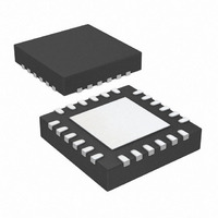
MCP23018-E/MJ Microchip Technology, MCP23018-E/MJ Datasheet - Page 10

MCP23018-E/MJ
Manufacturer Part Number
MCP23018-E/MJ
Description
IC I/O EXPANDER I2C 16B 24QFN
Manufacturer
Microchip Technology
Datasheet
1.MCP23018-ESO.pdf
(56 pages)
Specifications of MCP23018-E/MJ
Package / Case
24-QFN
Interface
I²C
Number Of I /o
16
Interrupt Output
Yes
Frequency - Clock
3.4MHz
Voltage - Supply
1.8 V ~ 5.5 V
Operating Temperature
-40°C ~ 125°C
Mounting Type
Surface Mount
Logic Family
MCP23018
Propagation Delay Time
50 ns
Operating Supply Voltage
1.8 V to 5.5 V
Power Dissipation
700 mW
Operating Temperature Range
- 40 C to + 125 C
Input Voltage
1.8 V to 5.5 V
Logic Type
I/O Expander
Maximum Clock Frequency
10 MHz
Maximum Operating Frequency
3.4 MHz
Mounting Style
SMD/SMT
Output Current
25 mA
Output Voltage
1.8 V to 4.5 V
Lead Free Status / RoHS Status
Lead free / RoHS Compliant
Lead Free Status / RoHS Status
Lead free / RoHS Compliant, Lead free / RoHS Compliant
Available stocks
Company
Part Number
Manufacturer
Quantity
Price
Company:
Part Number:
MCP23018-E/MJ
Manufacturer:
Microchip
Quantity:
1 195
Part Number:
MCP23018-E/MJ
Manufacturer:
MICROCHIP/微芯
Quantity:
20 000
MCP23018/MCP23S18
1.4
The ADDR pin is used to set the slave address of the
MCP23018 (I
the bus using only a single pin. Typically, this would
require three pins.
The multi-bit Address Decoder employs a basic FLASH
ADC architecture
generate 8 unique values based on the analog input.
This value is converted to a 3-bit code which corre-
sponds to the address bits (A2, A1, A0) in the serial
OPCODE.
Sequence
timings):
1.
FIGURE 1-2:
DS22103A-page 10
Upon power up (after V
becomes active after time t
log value on the ADDR pin must be stable
before this point to ensure accurate address
assignment.
Multi-bit Address Decoder
of
2
C only) to allow up to eight devices on
R1
R2
(Figure
V2
Operation
V
DD
VOLTAGE DIVIDER EXAMPLE
V
1-4). The seven comparators
SS
DD
ADDR
stabilizes) the module
(see
ADEN
. Note, the ana-
Figure 1-5
V
V
SS
DD
for
2.
3.
Once the address bits are latched, the device will keep
the slave address until a POR or reset condition
occurs.
1.4.1
When calculating the required voltage on the ADDR pin
(V2), the set point should be the mid-point of the LSb of
the ADC.
The examples in
to determine the mid point voltage (V2) and the range
of voltages based on a voltage divider circuit. The
maximum tolerance is 20%, however, it is recom-
mended to use 5% tolerance worst case (10% total tol-
erance).
MCP23018
The 3-bit address is latched after t
The module powers down after the first rising
edge of the serial clock is detected (t
CALCULATING VOLTAGE ON ADDR
Figure 1-2
© 2008 Microchip Technology Inc.
and
A0
A1
A2
Figure 1-3
ADDRLAT .
ADDIS
show how
).


