SI2493-C-FS Silicon Laboratories Inc, SI2493-C-FS Datasheet - Page 172

SI2493-C-FS
Manufacturer Part Number
SI2493-C-FS
Description
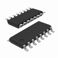
IC ISOMODEM SYSTEM-SIDE 16SOIC
Manufacturer
Silicon Laboratories Inc
Specifications of SI2493-C-FS
Mfg Application Notes
SI2493/57/34/15/04, Appl Note AN93
Data Format
V.21, V.22, V.23, V.29, V.32, V.34, V.90, V.92, Bell 103, Bell 212A
Baud Rates
56k
Interface
UART
Voltage - Supply
3 V ~ 3.6 V
Mounting Type
Surface Mount
Package / Case
16-SOIC (3.9mm Width)
Lead Free Status / RoHS Status
Lead free / RoHS Compliant
Available stocks
Company
Part Number
Manufacturer
Quantity
Price
Company:
Part Number:
SI2493-C-FSR
Manufacturer:
DY
Quantity:
8 623
Part Number:
SI2493-C-FSR
Manufacturer:
SIEMENS/西门子
Quantity:
20 000
- Current page: 172 of 230
- Download datasheet (7Mb)
AN93
172
10
12
13
14
15
16
17
18
19
20
21
22
23
24
25
26
27
28
11
#
1
2
3
4
5
6
7
8
9
Place U1 and U3 so pins 9-16 of U1 are facing pins 1-4 of U3
Place U1, U3, C1 and C2 to provide minimum required creepage distance
Place R12 and R13 close to U1
Place C1 and C2 directly between U1 and U3, connect with short direct traces
Place R7, R8, R18, and R19 and C11 close to U2, keeping away from U3 pins 1 and 2
Provide large collector pads for heat sinking Q2 and Q3.
Use >15 mil trace widths in DAA section and >20 mil IGND trace widths
Place C3 directly across D1 and minimize IGND trace length
Place FB1, FB2, R15, R16, and RV1 close to the RJ-11 jack
Place C8 and C9 to minimize trace length to chassis ground
The traces from the RJ-11 through C8 and C9 to chassis ground must be short
Keep C8 and C9 away from C1 and C2 or place at 90 degrees
Use >20mil trace widths between RJ-11, FB1-2, R15, R16, RV1 C8 and C9
Match the routing from the RJ-11 to FB1 and FB2
Match traces from FB1, R7, C11 to U3 to those from FB2, R8, R18 to U3
There must be no digital ground or power plane in DAA area
Place C4 close to U2 and connect with very short direct traces
>5 mm creepage between any TNV and SELV component, pad or trace
Mark U1 pin 1 and U3 pin1
Allow space and mounting holes for fire enclosure if required
IGND plane does NOT extend under C3, D1, FB1-2, R15-16, C8-9 or RV1
All traces connecting C50, C51, C52 and U1 must be short and direct
The XTALI, Y1, XTALO loop must be minimized and routed on one layer
The Y1, C40, C41 loop must be minimized and routed on one layer
No traces can be routed through the Y1, C40, C41 loop
Space U2, Q1, Q2, Q3, R1, R2, and R10 for best thermal performance.
Size Q1, Q2, and Q3 collector pads to safely dissipate 0.15 W (see text).
Submit layout to Silicon Laboratories for review
Table 110. Si2493/57/34/15/04/Si3008 Layout Checklist
Layout Requirement
Rev. 0.9
Related parts for SI2493-C-FS
Image
Part Number
Description
Manufacturer
Datasheet
Request
R
Part Number:
Description:
SOIC 16/C�/56 KBPS, V.92 ISOMODEM 16-PIN SYSTEM-SIDE - LEAD-FREE
Manufacturer:
Silicon Laboratories Inc
Part Number:
Description:
TSSOP 24/I�/56 KBPS, V.92 ISOMODEM SYSTEM-SIDE
Manufacturer:
Silicon Laboratories Inc
Part Number:
Description:
IC ISOMODEM SYSTEM-SIDE 24TSSOP
Manufacturer:
Silicon Laboratories Inc
Datasheet:
Part Number:
Description:
56 KBPS, V.92 ISOMODEM SYSTEM-SIDE - LEAD-FREE TSSOP 0 TO 7
Manufacturer:
Silicon Laboratories Inc
Datasheet:
Part Number:
Description:
Telecom ICs CONTACT SILICON LABS FOR AVAILABILITY
Manufacturer:
Silicon Laboratories Inc
Part Number:
Description:
IC ISOMODEM SYSTEM-SIDE 16SOIC
Manufacturer:
Silicon Laboratories Inc
Datasheet:
Part Number:
Description:
IC ISOMODEM SYSTEM-SIDE 24TSSOP
Manufacturer:
Silicon Laboratories Inc
Datasheet:

Part Number:
Description:
IC ISOMODEM W/ERROR CORR 16SOIC
Manufacturer:
Silicon Laboratories Inc
Datasheet:
Part Number:
Description:
IC ISOMODEM W/ERROR CORR 24TSSOP
Manufacturer:
Silicon Laboratories Inc
Datasheet:

Part Number:
Description:
IC ISOMODEM W/DAA 16SOIC
Manufacturer:
Silicon Laboratories Inc
Datasheet:
Part Number:
Description:
IC ISOMODEM SYSTEM-SIDE 24TSSOP
Manufacturer:
Silicon Laboratories Inc
Datasheet:
Part Number:
Description:
IC ISOMODEM W/ERROR CORR 24TSSOP
Manufacturer:
Silicon Laboratories Inc
Datasheet:
Part Number:
Description:
IC ISOMODEM W/DAA 24TSSOP
Manufacturer:
Silicon Laboratories Inc
Datasheet:


