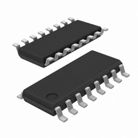
SI2493-C-FS Silicon Laboratories Inc, SI2493-C-FS Datasheet - Page 86

SI2493-C-FS
Manufacturer Part Number
SI2493-C-FS
Description
IC ISOMODEM SYSTEM-SIDE 16SOIC
Manufacturer
Silicon Laboratories Inc
Specifications of SI2493-C-FS
Mfg Application Notes
SI2493/57/34/15/04, Appl Note AN93
Data Format
V.21, V.22, V.23, V.29, V.32, V.34, V.90, V.92, Bell 103, Bell 212A
Baud Rates
56k
Interface
UART
Voltage - Supply
3 V ~ 3.6 V
Mounting Type
Surface Mount
Package / Case
16-SOIC (3.9mm Width)
Lead Free Status / RoHS Status
Lead free / RoHS Compliant
Available stocks
Company
Part Number
Manufacturer
Quantity
Price
Company:
Part Number:
SI2493-C-FSR
Manufacturer:
DY
Quantity:
8 623
Part Number:
SI2493-C-FSR
Manufacturer:
SIEMENS/西门子
Quantity:
20 000
- Current page: 86 of 230
- Download datasheet (7Mb)
AN93
3.3.29. U65 (DAAC4)
U65 (DAAC4) is a bit-mapped register with bits 3:0,
12:5, and 15 reserved. Bits 1:0 and 6:5 must not be
changed in a read-modify-write cycle.
Bit 14 (PWMG) = 0 (default) provides 0 dB gain to
AOUT. PWMG = 1 provides a 6 dB gain to AOUT.
Bit 13 (PDN) = 0 allows the device to operate at normal
power level. PDN = 1 completely powers down both the
Si3018/10 and the Si2493/57/34/15/04 chips.
3.3.30. U66 (DAA Control Register 5, DAAC5)
U66 (DAAC5) is a bit-mapped register with all bits
except bit 6 reserved (see Table 53).
Bit 6 (FDT) is a read-only bit that reports whether or not
an isolation capacitor frame lock is established. FDT is
typically used for board-level debugging and is not used
during normal modem operation.
U66 resets to 0xXX40 with a power-on or manual reset
assuming framelock is established. The upper byte is
variable.
86
12:7
6:5
3:2
1:0
Bit
15
14
13
4
Reserved Read returns zero.
Reserved Read returns zero.
Reserved Must not change in a read-modify-write.
Reserved Read returns zero.
Reserved Must not change in a read-modify-write.
PWMG
Name
PDN
PDL
Function
PWM Gain.
0 = No gain.
1 = 6 dB gain applied to AOUT.
Powerdown.
0 = Normal.
1 = Powerdown.
Powerdown Line-Side Chip.
0 = Normal operation.
1 = Places the Si3018/10 in powerdown mode.
Table 52. U65 Bit Map
Rev. 0.9
The bit takes effect at the carriage return of the AT
command writing this bit to a 1. Once this bit is set, the
modem must be reset via the RESET pin (Si2493/57/
34/15/04, pin 12) to become active. When reset, the
modem reverts to the default settings.
Bit 4 (PDL) = 0 (default) allows the modem to operate at
normal power levels. PDL = 1 powers down the Si3018/
103018/10. This is a test mode typically used for board-
level debugging, not normal modem operation.
U65 resets to 0x00E0 with a power-on or manual reset.
3.3.31. U67–U6A (International Configuration Regis-
International Configuration Registers include U67
through U6A. These are bit-mapped registers that
control international configuration settings, such as dc
and ac termination, ringer impedance and detection,
current limit, and billing tone protection.
3.3.32. U67 (ITC1)
U67 is a bit-mapped register with bits 5:4, 8, 11:10, and
15:14 reserved (see Table 54). U67 resets to 0x0008
with a power-on or manual reset.
Bit 7 (DCR) is used to set the dc line termination of the
modem. DCR = 0
dc impedance selected by U67[3:2] (DCV).
ters)
b
is the normal mode of operation with
Related parts for SI2493-C-FS
Image
Part Number
Description
Manufacturer
Datasheet
Request
R
Part Number:
Description:
SOIC 16/C�/56 KBPS, V.92 ISOMODEM 16-PIN SYSTEM-SIDE - LEAD-FREE
Manufacturer:
Silicon Laboratories Inc
Part Number:
Description:
TSSOP 24/I�/56 KBPS, V.92 ISOMODEM SYSTEM-SIDE
Manufacturer:
Silicon Laboratories Inc
Part Number:
Description:
IC ISOMODEM SYSTEM-SIDE 24TSSOP
Manufacturer:
Silicon Laboratories Inc
Datasheet:
Part Number:
Description:
56 KBPS, V.92 ISOMODEM SYSTEM-SIDE - LEAD-FREE TSSOP 0 TO 7
Manufacturer:
Silicon Laboratories Inc
Datasheet:
Part Number:
Description:
Telecom ICs CONTACT SILICON LABS FOR AVAILABILITY
Manufacturer:
Silicon Laboratories Inc
Part Number:
Description:
IC ISOMODEM SYSTEM-SIDE 16SOIC
Manufacturer:
Silicon Laboratories Inc
Datasheet:
Part Number:
Description:
IC ISOMODEM SYSTEM-SIDE 24TSSOP
Manufacturer:
Silicon Laboratories Inc
Datasheet:

Part Number:
Description:
IC ISOMODEM W/ERROR CORR 16SOIC
Manufacturer:
Silicon Laboratories Inc
Datasheet:
Part Number:
Description:
IC ISOMODEM W/ERROR CORR 24TSSOP
Manufacturer:
Silicon Laboratories Inc
Datasheet:

Part Number:
Description:
IC ISOMODEM W/DAA 16SOIC
Manufacturer:
Silicon Laboratories Inc
Datasheet:
Part Number:
Description:
IC ISOMODEM SYSTEM-SIDE 24TSSOP
Manufacturer:
Silicon Laboratories Inc
Datasheet:
Part Number:
Description:
IC ISOMODEM W/ERROR CORR 24TSSOP
Manufacturer:
Silicon Laboratories Inc
Datasheet:
Part Number:
Description:
IC ISOMODEM W/DAA 24TSSOP
Manufacturer:
Silicon Laboratories Inc
Datasheet:


