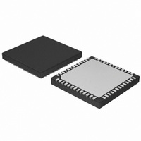
AMIS49587C5872G ON Semiconductor, AMIS49587C5872G Datasheet - Page 10

AMIS49587C5872G
Manufacturer Part Number
AMIS49587C5872G
Description
IC MODEM PLC 50/60MHZ 52QFN
Manufacturer
ON Semiconductor
Datasheet
1.AMIS49587C5871RG.pdf
(55 pages)
Specifications of AMIS49587C5872G
Baud Rates
Selectable
Interface
SCI
Voltage - Supply
3 V ~ 3.6 V
Mounting Type
Surface Mount
Package / Case
52-TQFN Exposed Pad
Maximum Operating Temperature
+ 80 C
Minimum Operating Temperature
- 40 C
Modulation Type
.
Mounting Style
SMD/SMT
Operating Supply Voltage
+ 3 V to 3.6 V
Number Of Transmitters
1
Power Supply Requirement
Single
Package Type
QFN EP
Operating Temperature Classification
Commercial
Mounting
Surface Mount
Pin Count
52
Operating Temperature (min)
-40C
Dual Supply Voltage (typ)
Not RequiredV
Dual Supply Voltage (max)
Not RequiredV
Dual Supply Voltage (min)
Not RequiredV
Lead Free Status / RoHS Status
Lead free / RoHS Compliant
Data Format
-
Lead Free Status / Rohs Status
Compliant
AMIS- -49587
CRC
CRC is a 5V compliant open drain output. An external pull- -up resistor defines the logic high level as illustrated in Figure 5.
A typical value for this pull- -up resistance “R” is 10 kΩ. The signal on this output depends on the cyclic redundancy code result
of the received frame. If the cyclic redundancy code is correct CRC = 1 during the pause between 2 time slots.
RESB
RESB is a digital input pin. It is used to perform a hardware reset of the AMIS- -49587. This pin supports a 5 V voltage level.
The reset is active when the signal is low (0 V).
TEST
TEST is a digital input pin. It is used to enable the test mode of the chip. Normal mode is activated when TEST signal is low
(0 V). For normal operation, the TEST pin may be left unconnected. Due to the internal pulldown, the signal is maintained
to low (0 V). TEST pin is not 5 V safe.
TX_ENB
TX_ENB is a digital output pin. It is low when the transmitter is activated. The signal is available to turn on the line driver.
TX_ENB is a 5 V safe with open drain output, hence a pull- -up resistance is necessary achieve the requested voltage level
associated with a logical one. See also Figure 5 for reference.
TX_OUT
TX_OUT is the analog output pin of the transmitter. The provided signal is the S- -FSK modulated frames. A filtering operation
must be performed to reduce the second order harmonic distortion. For this purpose an active filter is realized. Figure 7 gives
the representation of this filter.
Transmitter (S--FSK Modulator)
C
ALC _IN
ALC
4
FROM LINE
control
DRIVER
R
3
ARM
C
3
Interface
C
&
R
R
1
LP
2
1
TX_OUT
Control
Filter
C
2
TX_EN
TO TX POWER
OUTPUT STAGE
V
SSA
Figure 7. TX_OUT Filter
ALC_IN
ALC_IN is the automatic level control analog input pin. The signal is used to adjust the level of the transmitted signal. The
signal level adaptation is based on the AC component. The DC level on the ALC_IN pin is fixed internally to 1.65 V.
Comparing the peak voltage of the AC signal with two internal thresholds does the adaptation of the gain. Low threshold is
fixed to 0.4 V. A value under this threshold will result in an increase of the gain. The high threshold is fixed to 0.6 V. A value
over this threshold will result in a decrease of the gain. A serial capacitance is used to block the DC components. The level
adaptation is performed during the transmission of the first two bits of a new frame. Eight successive adaptations are
performed.
http://onsemi.com
10


