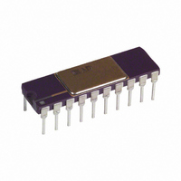
AD693AQ Analog Devices Inc, AD693AQ Datasheet - Page 11

AD693AQ
Manufacturer Part Number
AD693AQ
Description
IC TRANSMITTER 4-20MA 20-CDIP
Manufacturer
Analog Devices Inc
Type
Signal Conditionerr
Datasheet
1.AD693AQ.pdf
(12 pages)
Specifications of AD693AQ
Rohs Status
RoHS non-compliant
Input Type
Voltage
Output Type
Voltage
Interface
3-Wire
Current - Supply
20mA
Mounting Type
Through Hole
Package / Case
20-CDIP (0.300", 7.62mm)
Supply Voltage Range
12V To 36V
Operating Temperature Range
-40°C To +85°C
Digital Ic Case Style
DIP
No. Of Pins
20
Svhc
No SVHC (18-Jun-2010)
Operating Temperature Max
85°C
Operating
RoHS Compliant
Converter Type
Voltage to Current
Current, Output
+25 mA (Typ.)
Current, Quiescent Supply
+500 uA (Typ.)
Package Type
Cerdip
Temperature, Operating, Maximum
85 °C
Temperature, Operating, Minimum
-40 °C
Voltage, Operating
+12 V (Min.)
No. Of Amplifiers
5
Input Offset Voltage
200µV
Cmrr
90dB
Supply Current
500µA
Amplifier Case Style
DIP
Rohs Compliant
No
Ic Function
Sensor Transmitter
Amplifier Type
Current
Base Number
693
Lead Free Status / RoHS Status
Available stocks
Company
Part Number
Manufacturer
Quantity
Price
Company:
Part Number:
AD693AQ
Manufacturer:
TOSHIBA
Quantity:
101
Part Number:
AD693AQ
Manufacturer:
ADI/亚德诺
Quantity:
20 000
REV. A
via a set of thermocouple tables referenced to C. For example,
the output of a properly referenced type J thermocouple is
60 mV when the hot junction is at 1035 C. Table II lists the
maximum measurement temperature for several thermocouple
types using the preadjusted 30 mV and 60 mV input ranges.
More convenient temperature ranges can be selected by deter-
mining the full-scale input voltages via standard thermocouple
tables and adjusting the AD693 span. For example, suppose
only a 300 C span is to be measured with a type K thermo-
couple. From a standard table, the thermocouple output is
12.207 mV; since 60 mV at the signal amplifier corresponds to a
16 mA span at the output a gain of 5, or more precisely 60 mV/
12.207 mV = 4.915 will be needed. Using a 12.207 mV span in
the gain resistor formula given in “Adjusting Input Span” yields
a value of about 270
a 50
With the connection illustrated, the AD693 will give a full-scale
indication with an open thermocouple.
ERROR BUDGET ANALYSIS
Loop-Powered Operation specifications refer to parameters
tested with the AD693 operating as a loop-powered transmitter.
The specifications are valid for the preset spans of 30 mV,
60 mV and those spans in between. The section, “Components
of Error,” refers to parameters tested on the individual functional
blocks, (Signal Amplifier, V/I Converter, Voltage Reference, and
Auxiliary Amplifier). These can be used to get an indication of
device performance when the AD693 is used in local power
mode or when it is adjusted to spans of less than 30 mV.
potentiometer will allow ample adjustment range.
POLARITY
+
–
+
_
+
–
+
–
as the minimum from P1 to 6.2 V. Adding
MATERIAL
IRON
CONSTANTAN
NICKEL-CHROME
NICKEL-ALUMINUM
NICKEL-CHROME
COPPER-NICKEL
COPPER
COPPER-NICKEL
Figure 19. Thermocouple Inputs with Cold Junction Compensation
Table II. Thermocouple Application—Cold Junction Compensation
TYPE
J
K
E
T
AMBIENT
TEMP
25
75
25
75
25
75
25
75
–11–
Table III lists the expressions required to calculate the total
error. The AD693 is tested with a 250
RTI Contributions to Offset Error
I
PSRR Power Supply Rejection Ratio
CMRR Common-Mode Rejection Ratio |V
IOS
RTI Contributions to Span Error
X
X
X
X
I
Abbreviations
I
I
R
R
V
V
V
X
1
2
RCOMP
ZE
DIFF
Z
S
The 4–20 mA signal, flowing through the metering resistor, modulates the power supply voltage seen
The input bias current of the inverting input increases with input signal voltage. The differential
by the AD693. The change in voltage causes a power supply rejection error that varies with the
output current, thus it appears as a span error.
input current, I
Figure 2. I
ies with signal. If the change in differential input current with input signal is approximated as a
linear function, then any error due to source impedance may be approximated as a span error. To
calculate I
input voltage for your application. Multiply by + In max to get I
impedance to get the input voltage error at full scale.
51.7
53.6
40.2
42.2
60.4
64.9
40.2
45.3
S
L
LOOP
CM
SPAN
SE
PSRR
CMRR
NL
S
Table III. RTI Contributions to Span and Offset Error
Error Source
Zero Current Error
Input Offset Current
Error Source
Transconductance Error
Transconductance PSRR
Transconductance CMRR
Nonlinearity
Differential Input Current
Zero Current (usually 4 mA)
Output span (usually 16 mA)
Input source impedance
Load resistance
Loop supply voltage
Input common-mode voltage
Input span
Nominal transconductance in A/V
DIFF
DIFF
, refer to Figure 2 and find the value for I
, flowing into an input source impedance, will cause an input voltage error that var-
RZ
301K
294K
392K
374K
261K
243K
392K
340K
DIFF
, equals the inverting input current minus the noninverting input current; see
RANGE
USE WITH GAIN >2
30 mV
TEMP
546 C
721 C
413 C
1
2
RANGE
1035 C
787 C
60 mV
TEMP
—
Expression for RTI Error at Zero
I
R
Expression for RTI Error at Full Scale
V
|R
|V
V
RS
(|V
ZE
S
SPAN
SPAN
/X
CM
L
CM
LOOP
– 250 |
IOS
S
I
– 3.1 V|
– 3.1 V|
DIFF
– 24 V| + [|R
X
DIFF
X
SE
NL
/ + In corresponding to the full-scale
load, a 24 V loop supply
I
DlFF
CMRR
S
V
SPAN
. Multiply I
PSRR
L
– 250 | I
AD693
X
CMRR
DIFF
by the source
Z
]) PSRR


