AD693AQ Analog Devices Inc, AD693AQ Datasheet - Page 6
AD693AQ
Manufacturer Part Number
AD693AQ
Description
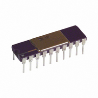
IC TRANSMITTER 4-20MA 20-CDIP
Manufacturer
Analog Devices Inc
Type
Signal Conditionerr
Datasheet
1.AD693AQ.pdf
(12 pages)
Specifications of AD693AQ
Rohs Status
RoHS non-compliant
Input Type
Voltage
Output Type
Voltage
Interface
3-Wire
Current - Supply
20mA
Mounting Type
Through Hole
Package / Case
20-CDIP (0.300", 7.62mm)
Supply Voltage Range
12V To 36V
Operating Temperature Range
-40°C To +85°C
Digital Ic Case Style
DIP
No. Of Pins
20
Svhc
No SVHC (18-Jun-2010)
Operating Temperature Max
85°C
Operating
RoHS Compliant
Converter Type
Voltage to Current
Current, Output
+25 mA (Typ.)
Current, Quiescent Supply
+500 uA (Typ.)
Package Type
Cerdip
Temperature, Operating, Maximum
85 °C
Temperature, Operating, Minimum
-40 °C
Voltage, Operating
+12 V (Min.)
No. Of Amplifiers
5
Input Offset Voltage
200µV
Cmrr
90dB
Supply Current
500µA
Amplifier Case Style
DIP
Rohs Compliant
No
Ic Function
Sensor Transmitter
Amplifier Type
Current
Base Number
693
Lead Free Status / RoHS Status
Available stocks
Company
Part Number
Manufacturer
Quantity
Price
Company:

Part Number:
AD693AQ
Manufacturer:
TOSHIBA
Quantity:
101
Part Number:
AD693AQ
Manufacturer:
ADI/亚德诺
Quantity:
20 000


AD693
if the 6.2 V of the reference is unsuitable. Configured as a simple
follower, it can be driven from a user supplied voltage divider
or the precalibrated outputs of the AD693 divider (Pins 3 and
4) to provide a stiff voltage output at less than the 6.2 level, or
by incorporating a voltage divider as feedback around the amplifier,
one can gain-up the reference to levels higher than 6.2 V. If
large positive outputs are desired, I
output current supply, should be strapped to either V
Boost. Like the Signal Amplifier, the Auxiliary requires about
3.5 V of headroom with respect to V
of difference between I
to swing.
The output stage of the Auxiliary Amplifier is actually a high
gain Darlington transistor where I
emitter. Thus, the Auxiliary Amplifier can be used as a V/I
converter when configured as a follower and resistively loaded.
I
is equal to the voltage at V
example, using the onboard 100
150 mV application voltages, either a 750 A or 1.5 mA current
source can be set up for transducer excitation.
The I
Auxiliary Amplifier is not to be used, then Pin 2, the noninverting
input, should be grounded.
REVERSE VOLTAGE PROTECTION FEATURE
In the event of a reverse voltage being applied to the AD693
through a current-limited loop (limited to 200 mA), an internal
shunt diode protects the device from damage. This protection
mode avoids the compliance voltage penalty which results from
a series diode that must be added if reversal protection is
required in high-current loops.
Applying the AD693
CONNECTIONS FOR BASIC OPERATION
Figure 10 shows the minimal connections for basic operation:
0–30 mV input span, 4–20 mA output span in the two-wire,
loop-powered mode. If not used for external excitation, the
6.2 V reference should be loaded by approximately 1 mA
(6.2 k to common).
X
functions as a high-impedance current source whose current
X
terminal has voltage compliance within 2 V of V
X
and the voltage to which V
Figure 10. Minimal Connection for 0–30 mV Unipolar Input, 4–20 mA Output
X
divided by the load resistance. For
X
X
, the Auxiliary Amplifier
resistor and the 75 mV or
is the collector and V
IN
at its input and about 2 V
X
X
IN
is required
. If the
or
X
is the
–6–
USING AN EXTERNAL PASS TRANSISTOR
The emitter of the NPN output section, I
usually connected to common and the negative loop connection
(Pins 7 to 6). Provision has been made to reconnect I
base of a user supplied NPN transistor as shown in Figure 11.
This permits the majority of the power dissipation to be moved
off chip to enhance performance, improve reliability, and extend
the operating temperature range. An internal hold-down resistor
of about 3k is connected across the base emitter of the external
transistor.
The external pass transistor selected should have a BV
than the intended supply voltage with a sufficient power rating for
continuous operation with 25 mA current at the supply voltage.
Ft should be in the 10 MHz to 100 MHz range and
greater than 10 at a 20 mA emitter current. Some transistors
that meet this criteria are the 2N1711 and 2N2219A. Heat
sinking the external pass transistor is suggested.
The pass transistor option may also be employed for other
applications as well. For example, I
LED connected to Common, thus providing a local monitor of
loop fault conditions without reducing the minimum compliance
voltage.
ADJUSTING ZERO
In general, the desired zero offset value is obtained by
connecting an appropriate tap of the precision reference/voltage
divider network to the inverting terminal of the V/I converter.
As shown in Figure 9, precalibrated taps at Pins 14, 13 and 11
result in zero offsets of 0 mA, 4 mA and 12 mA, respectively,
when connected to Pin 12. The voltages which set the 4 mA and
12 mA zero operating points are 15 mV and 45 mV negative
with respect to 6.2 V, and they each have a nominal source
resistance of 450 . While these voltages are laser trimmed to
high accuracy, they may require some adjustment to
accommodate variability between sensors or to provide
additional ranges. You can adjust zero by pulling up or down on
the selected zero tap, or by making a separate voltage divider to
drive the zero pin.
The arrangement of Figure 12 will give an approximately linear
adjustment of the precalibrated options with fixed limits. To
find the proper resistor values, first select I
OUT
can be used to drive an
OUT
A
, the desired range
, of the AD693 is
CEO
OUT
should be
greater
REV. A
to the
Related parts for AD693AQ
Image
Part Number
Description
Manufacturer
Datasheet
Request
R

Part Number:
Description:
±1.7g Dual-Axis IMEMS Accelerometer Evaluation Board
Manufacturer:
Analog Devices Inc
Datasheet:

Part Number:
Description:
Inertial Sensor Evaluation System
Manufacturer:
Analog Devices Inc
Datasheet:
Part Number:
Description:
Manufacturer:
Analog Devices Inc
Datasheet:
Part Number:
Description:
Manufacturer:
Analog Devices Inc
Datasheet:
Part Number:
Description:
Manufacturer:
Analog Devices Inc
Datasheet:
Part Number:
Description:
Manufacturer:
Analog Devices Inc
Datasheet:
Part Number:
Description:
Manufacturer:
Analog Devices Inc
Datasheet:
Part Number:
Description:
Manufacturer:
Analog Devices Inc
Datasheet:
Part Number:
Description:
Manufacturer:
Analog Devices Inc
Datasheet:
Part Number:
Description:
Manufacturer:
Analog Devices Inc
Datasheet:
Part Number:
Description:
Manufacturer:
Analog Devices Inc
Datasheet:
Part Number:
Description:
Manufacturer:
Analog Devices Inc
Datasheet:
Part Number:
Description:
Manufacturer:
Analog Devices Inc
Datasheet: