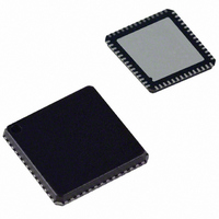
AD9995KCPZRL Analog Devices Inc, AD9995KCPZRL Datasheet - Page 20

AD9995KCPZRL
Manufacturer Part Number
AD9995KCPZRL
Description
IC CCD SIGNAL PROCESSOR 56-LFCSP
Manufacturer
Analog Devices Inc
Type
CCD Signal Processor, 12-Bitr
Datasheet
1.AD9995KCPZRL.pdf
(60 pages)
Specifications of AD9995KCPZRL
Input Type
Logic
Output Type
Logic
Interface
3-Wire Serial
Current - Supply
30mA
Mounting Type
Surface Mount
Package / Case
56-LFCSP
Analog Front End Type
CCD
Analog Front End Category
Video
Interface Type
Serial (3-Wire)
Input Voltage Range
0.5V
Operating Supply Voltage (min)
2.7V
Operating Supply Voltage (typ)
3V
Operating Supply Voltage (max)
3.6V
Resolution
12b
Number Of Adc's
1
Power Supply Type
Analog/Digital
Operating Temp Range
-20C to 85C
Operating Temperature Classification
Commercial
Mounting
Surface Mount
Pin Count
56
Package Type
LFCSP EP
Number Of Channels
1
Lead Free Status / RoHS Status
Lead free / RoHS Compliant
Available stocks
Company
Part Number
Manufacturer
Quantity
Price
Company:
Part Number:
AD9995KCPZRL7
Manufacturer:
SANYO
Quantity:
1 170
HBLK
Generating Line Alternation for V-Sequence and HBLK
During low resolution readout, some CCDs require a different
number of vertical clocks on alternate lines. The AD9995 can
support this by using the VPATREPO and VPATREPE regis-
ters. This allows a different number of VPAT repetitions to be
programmed on odd and even lines. Note that only the number
of repeats can be different in odd and even lines, but the VPAT
group remains the same.
Additionally, the HBLK signal can also be alternated for odd
and even lines. When the HBLKALT register is set high, the
HBLK TOG1 and TOG2 positions will be used on odd lines
and the TOG3–TOG6 positions will be used on even lines.
This allows the HBLK interval to be adjusted on odd and even
lines if needed.
Figure 19 shows an example of VPAT repetition alternation and
HBLK alternation used together. It is also possible to use VPAT
and HBLK alternation separately.
AD9995
HD
V1
V2
V6
NOTES
1. THE NUMBER OF REPEATS FOR THE V-PATTERN GROUP MAY BE ALTERNATED ON ODD AND EVEN LINES.
2. THE HBLK TOGGLE POSITIONS MAY BE ALTERNATED BETWEEN ODD AND EVEN LINES IN ORDER TO GENERATE DIFFERENT HBLK PATTERNS FOR ODD/EVEN LINES.
VSG
HD
V2
V6
V1
TOG1
VPATREPO = 2
Figure 19. Odd/Even Line Alternation of VPAT Repetitions and HBLKToggle Positions
TOG2
Figure 20. Example of Second VPAT Group during Sensor Gate Line
TOG3
VPATREPE = 5
START POSITION FOR 2ND VPAT GROUP
USES VPATLEN REGISTER
–20–
Second V-Pattern Group during VSG Active Line
Most CCDs require additional vertical timing during the sensor
gate line. The AD9995 supports the option to output a second
V-pattern group for V1–V6 during the line when the sensor gates
VSG1–VSG5 are active. Figure 20 shows a typical VSG line, which
includes two separate sets of V-pattern groups for V1–V6. The
V-pattern group at the start of the VSG line is selected in the same
manner as the other regions, using the appropriate VSEQSEL
register. The second V-pattern group, unique to the VSG line, is
selected using the VPATSECOND register, located with the Field
registers. The start position of the second VPAT group uses the
VPATLEN register from the selected VPAT registers. Because
the VPATLEN register is used as the start position and not as the
VPAT length, it is not possible to program multiple repetitions
for the second VPAT group.
TOG4
2ND VPAT GROUP
TOG1
VPATREPO = 2
TOG2
REV. 0


