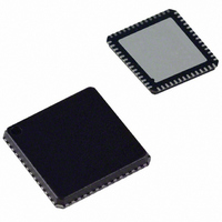
AD9995KCPZRL Analog Devices Inc, AD9995KCPZRL Datasheet - Page 29

AD9995KCPZRL
Manufacturer Part Number
AD9995KCPZRL
Description
IC CCD SIGNAL PROCESSOR 56-LFCSP
Manufacturer
Analog Devices Inc
Type
CCD Signal Processor, 12-Bitr
Datasheet
1.AD9995KCPZRL.pdf
(60 pages)
Specifications of AD9995KCPZRL
Input Type
Logic
Output Type
Logic
Interface
3-Wire Serial
Current - Supply
30mA
Mounting Type
Surface Mount
Package / Case
56-LFCSP
Analog Front End Type
CCD
Analog Front End Category
Video
Interface Type
Serial (3-Wire)
Input Voltage Range
0.5V
Operating Supply Voltage (min)
2.7V
Operating Supply Voltage (typ)
3V
Operating Supply Voltage (max)
3.6V
Resolution
12b
Number Of Adc's
1
Power Supply Type
Analog/Digital
Operating Temp Range
-20C to 85C
Operating Temperature Classification
Commercial
Mounting
Surface Mount
Pin Count
56
Package Type
LFCSP EP
Number Of Channels
1
Lead Free Status / RoHS Status
Lead free / RoHS Compliant
Available stocks
Company
Part Number
Manufacturer
Quantity
Price
Company:
Part Number:
AD9995KCPZRL7
Manufacturer:
SANYO
Quantity:
1 170
off positions. STROBON_FD is the field in which the STROBE
is turned on, measured from the field containing the last SUBCK
before exposure begins. The STROBON_ LN PX register gives
the line and pixel positions with respect to STROBON_FD. The
STROBE off position is programmable to any field, line, and
pixel location with respect to the field of the last SUBCK.
TRIGGER Register Limitations
While the TRIGGER register can be used to perform a complete
exposure and readout operation, there are limitations on its use.
Once an exposure-plus-readout operation has been triggered,
another exposure/readout operation cannot be triggered right
away. There must be at least one idle field (VD intervals) before
the next exposure/readout can be triggered.
Register
VSUBMODE[0]
VSUBMODE[1]
VSUBON[11:0]
VSUBON[12]
MSHUTPOL[0]
MSHUTPOL[1]
MSHUTON
MSHUTOFF_FD
MSHUTOFF_LNPX
STROBPOL
STROBON_FD
STROBON_LNPX
STROBOFF_FD
STROBOFF_LNPX
REV. 0
STROBE
SUBCK
VSG
VD
1
STROBE PROGRAMMABLE SETTINGS:
1. ACTIVE POLARITY.
2. ON POSITION IS PROGRAMMABLE IN ANY FIELD DURING THE EXPOSURE TIME (WITH RESPECT TO THE FIELD CONTAINING THE LAST SUBCK).
3. OFF POSITION IS PROGRAMMABLE IN ANY FIELD DURING THE EXPOSURE TIME.
Length
1b
1b
12b
1b
1b
1b
24b
12b
24b
1b
12b
24b
12b
24b
Table XII. VSUB, MSHUT, and STROBE Register Parameters
Range
High/Low
High/Low
0–4095 Line Location
High/Low
High/Low
On/Off
0–4095 Line/Pix Location
0–4095 Field Location
0–4095 Line/Pix Location
High/Low
0–4095 Field Location
0–4095 Line/Pix Location
0–4095 Field Location
0–4095 Line/Pix Location
AND STROBE
EXPOSURE
TRIGGER
Figure 31. STROBE Output Programmability
2
–29–
Description
VSUB Mode (0 = Mode 0, 1 = Mode 1) (See Figure 29).
VSUB Keep-On Mode. VSUB will stay active after readout
when set high.
VSUB On Position. Active starting in any line of field.
VSUB Active Polarity.
MSHUT Active Polarity.
MSHUT Manual Enable (1 = Active or Open).
MSHUT On Position Line [11:0] and Pixel [23:12] Location.
Field Location to Switch Off MSHUT (Inactive or Closed).
Line/Pixel Position to Switch Off MSHUT (Inactive or Closed).
STROBE Active Polarity.
STROBE ON Field Location, with Respect to Last SUBCK Field.
STROBE ON Line/Pixel Position.
STROBE OFF Field Location, with Respect to Last SUBCK Field.
STROBE OFF Line/Pixel Position.
The same limitation applies to the triggering of the MSHUT
signal. There must be at least one idle field after the completion
of the MSHUT OFF operation before another MSHUT OFF
operation may be programmed.
The VSUB trigger requires two idle fields between exposure/
readout operations in order to ensure proper VSUB on/off trig-
gering. If the VSUB signal is not required to be turned on and
off in between each successive exposure/readout operation, this
limitation can be ignored. The VSUB Keep-On mode is useful
when successive exposure/readout operations are required.
3
t
EXP
AD9995


