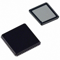
AD9995KCPZRL Analog Devices Inc, AD9995KCPZRL Datasheet - Page 52

AD9995KCPZRL
Manufacturer Part Number
AD9995KCPZRL
Description
IC CCD SIGNAL PROCESSOR 56-LFCSP
Manufacturer
Analog Devices Inc
Type
CCD Signal Processor, 12-Bitr
Datasheet
1.AD9995KCPZRL.pdf
(60 pages)
Specifications of AD9995KCPZRL
Input Type
Logic
Output Type
Logic
Interface
3-Wire Serial
Current - Supply
30mA
Mounting Type
Surface Mount
Package / Case
56-LFCSP
Analog Front End Type
CCD
Analog Front End Category
Video
Interface Type
Serial (3-Wire)
Input Voltage Range
0.5V
Operating Supply Voltage (min)
2.7V
Operating Supply Voltage (typ)
3V
Operating Supply Voltage (max)
3.6V
Resolution
12b
Number Of Adc's
1
Power Supply Type
Analog/Digital
Operating Temp Range
-20C to 85C
Operating Temperature Classification
Commercial
Mounting
Surface Mount
Pin Count
56
Package Type
LFCSP EP
Number Of Channels
1
Lead Free Status / RoHS Status
Lead free / RoHS Compliant
Available stocks
Company
Part Number
Manufacturer
Quantity
Price
Company:
Part Number:
AD9995KCPZRL7
Manufacturer:
SANYO
Quantity:
1 170
Address Content Value
A8
A9
AA
AB
AC
AD
AE
AF
Address Content Value
B0
B1
B2
B3
B4
B5
B6
B7
AD9995
Data Bit Default
[1:0]
[2]
[3]
[7:4]
[9:8]
[11:10]
[23:12]
[11:0]
[23:12]
[11:0]
[23:12]
[11:0]
[23:12]
[11:0]
[23:12]
[11:0]
[23:12]
[11:0]
[23:12]
[11:0]
[23:12]
Data Bit Default
[1:0]
[2]
[3]
[7:4]
[9:8]
[11:10]
[23:12]
[11:0]
[23:12]
[11:0]
[23:12]
[11:0]
[23:12]
[11:0]
[23:12]
[11:0]
[23:12]
[11:0]
[23:12]
[11:0]
[23:12]
0
0
0
0
0
0
0
0
0
0
0
0
0
0
0
0
0
0
0
0
0
0
0
0
0
0
0
0
0
0
0
0
0
0
0
0
0
0
0
0
0
0
Register Name
HBLKMASK_5
CLPOBPOL_5
CLPOBPOL_5
CLPOBPOL
PBLKPOL_5
PBLKPOL_5
PBLKPOL
VPATSEL_5
VPATSEL_5
VPATSEL
VMASK_5
VMASK_5
VMASK
HBLKALT_5
UNUSED
VPATREPO_5
VPATREPE_5
VPATSTART_5
HDLEN_5
PBLKTOG1_5
PBLKTOG2_5
HBLKTOG1_5
HBLKTOG2_5
HBLKTOG3_5
HBLKTOG4_5
HBLKTOG5_5
HBLKTOG6_5
CLPOBTOG1_5
CLPOBTOG2_5
Register Name
HBLKMASK_6
CLPOBPOL_6
CLPOBPOL_6
CLPOBPOL
PBLKPOL_6
PBLKPOL_6
PBLKPOL
VPATSEL_6
VPATSEL_6
VPATSEL
VMASK_6
VMASK_6
VMASK
HBLKALT_6
UNUSED
VPATREPO_6
VPATREPE_6
VPATSTART_6
HDLEN_6
PBLKTOG1_6
PBLKTOG2_6
HBLKTOG1_6
HBLKTOG2_6
HBLKTOG3_6
HBLKTOG4_6
HBLKTOG5_6
HBLKTOG6_6
CLPOBTOG1_6
CLPOBTOG2_6
Table XLIII. V-Sequence 6 (VSEQ6) Register Map
Table XLII. V-Sequence 5 (VSEQ5) Register Map
Description
Masking Polarity during HBLK. H1 [0]. H3 [1].
CLPOB Start Polarity
PBLK Start Polarity
Selected V-Pattern Group for V-Sequence 5
Enable Masking of V-Outputs (Specified by FREEZE/RESUME Registers)
Enable HBLK Alternation
Unused
Number of Selected V-Pattern Group Repetitions for Odd Lines
Number of Selected V-Pattern Group Repetitions for Even Lines
Start Position in the Line for the Selected V-Pattern Group
HD Line Length (Number of Pixels) for V-Sequence 5
PBLK Toggle Position 1 for V-Sequence 5
PBLK Toggle Position 2 for V-Sequence 5
HBLK Toggle Position 1 for V-Sequence 5
HBLK Toggle Position 2 for V-Sequence 5
HBLK Toggle Position 3 for V-Sequence 5
HBLK Toggle Position 4 for V-Sequence 5
HBLK Toggle Position 5 for V-Sequence 5
HBLK Toggle Position 6 for V-Sequence 5
CLPOB Toggle Position 1 for V-Sequence 5
CLPOB Toggle Position 2 for V-Sequence 5
Description
Masking Polarity during HBLK. H1 [0]. H3 [1].
CLPOB StartPolarity
PBLK Start Polarity
Selected V-Pattern Group for V-Sequence 6
Enable Masking of V-Outputs (Specified by FREEZE/RESUME Registers)
Enable HBLK Alternation
Unused
Number of Selected V-Pattern Group Repetitions for Odd Lines
Number of Selected V-Pattern Group Repetitions for Even Lines
Start Position in the Line for the Selected V-Pattern Group
HD Line Length (Number of Pixels) for V-Sequence 6
PBLK Toggle Position 1 for V-Sequence 6
PBLK Toggle Position 2 for V-Sequence 6
HBLK Toggle Position 1 for V-Sequence 6
HBLK Toggle Position 2 for V-Sequence 6
HBLK Toggle Position 3 for V-Sequence 6
HBLK Toggle Position 4 for V-Sequence 6
HBLK Toggle Position 5 for V-Sequence 6
HBLK Toggle Position 6 for V-Sequence 6
CLPOB Toggle Position 1 for V-Sequence 6
CLPOB Toggle Position 2 for V-Sequence 6
–52–
REV. 0


