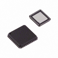
AD9949KCP Analog Devices Inc, AD9949KCP Datasheet - Page 4

AD9949KCP
Manufacturer Part Number
AD9949KCP
Description
IC CCD SIGNAL PROCESSOR 40-LFCSP
Manufacturer
Analog Devices Inc
Type
CCD Signal Processor, 12-Bitr
Datasheet
1.AD9949AKCPZ.pdf
(36 pages)
Specifications of AD9949KCP
Rohs Status
RoHS non-compliant
Input Type
Logic
Output Type
Logic
Interface
3-Wire Serial
Mounting Type
Surface Mount
Package / Case
40-LFCSP
Analog Front End Type
CCD
Analog Front End Category
Video
Interface Type
Serial (3-Wire)
Sample Rate
36MSPS
Input Voltage Range
0.5V
Operating Supply Voltage (min)
2.7V
Operating Supply Voltage (typ)
3V
Operating Supply Voltage (max)
3.6V
Resolution
12b
Number Of Adc's
1
Power Supply Type
Analog/Digital
Operating Temp Range
-20C to 85C
Operating Temperature Classification
Commercial
Mounting
Surface Mount
Pin Count
40
Package Type
LFCSP EP
Number Of Channels
1
Current - Supply
-
Lead Free Status / RoHS Status
Not Compliant
Available stocks
Company
Part Number
Manufacturer
Quantity
Price
Company:
Part Number:
AD9949KCP
Manufacturer:
AD
Quantity:
1 831
Company:
Part Number:
AD9949KCP
Manufacturer:
ADI
Quantity:
455
Company:
Part Number:
AD9949KCPZ
Manufacturer:
TI
Quantity:
6 528
Part Number:
AD9949KCPZ
Manufacturer:
ADI/亚德诺
Quantity:
20 000
Company:
Part Number:
AD9949KCPZRL
Manufacturer:
PERICOM
Quantity:
3
AD9949
ANALOG SPECIFICATIONS
T
Table 3.
Parameter
CDS
PIXEL GAIN AMPLIFIER (P×GA)
VARIABLE GAIN AMPLIFIER (VGA)
BLACK LEVEL CLAMP
A/D CONVERTER
VOLTAGE REFERENCE
SYSTEM PERFORMANCE
1
Input signal characteristics defined as follows:
RESET TRANSIENT
MIN
Gain
Allowable CCD Reset Transient
Maximum Input Range before Saturation
Maximum CCD Black Pixel Amplitude
Gain Control Resolution
Gain Monotonicity
Maximum Input Range
Maximum Output Range
Gain Control Resolution
Gain Monotonicity
Gain Range
Clamp Level Resolution
Clamp Level
Resolution
Differential Nonlinearity (DNL)
No Missing Codes
Integral Nonlinearity (INL)
Full-Scale Input Voltage
Reference Top Voltage (REFT)
Reference Bottom Voltage (REFB)
VGA Gain Accuracy
Peak Nonlinearity, 500 mV Input Signal
Total Output Noise
Power Supply Rejection (PSR)
500mV TYP
Minimum Gain
Maximum Gain
Minimum Gain (VGA Code 0)
Maximum Gain (VGA Code 1023)
Minimum Clamp Level (0)
Maximum Clamp Level (255)
Minimum Gain (Code 0)
Maximum Gain (Code 1023)
to T
MAX
OPTICAL BLACK PIXEL
, AVDD = DVDD = 3.0 V, f
50mV MAX
INPUT SIGNAL RANGE
1V MAX
1
1
CLI
= 36 MHz, typical timing specifications, unless otherwise noted.
1
Min
1.0
1.0
2.0
12
−1.0
5.0
40.5
Typ
0
500
±50
0
6
42
256
0
255
±0.5
2.0
1.0
5.5
41.5
0.15
0.8
256
18
1024
Guaranteed
Guaranteed
2.0
50
Rev. B | Page 4 of 36
Max
+1.0
8
6.0
42.5
0.6
Unit
dB
mV
V p-p
mV
Steps
dB
dB
V p-p
V p-p
Steps
dB
dB
Steps
LSB
LSB
Bits
LSB
LSB
V
V
V
dB
dB
%
LSB rms
dB
Notes
Measured at ADC output
Specifications include entire signal chain
12 dB gain applied
AC grounded input, 6 dB gain applied
Measured with step change on supply


