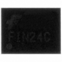
FIN24CGFX Fairchild Semiconductor, FIN24CGFX Datasheet - Page 3

FIN24CGFX
Manufacturer Part Number
FIN24CGFX
Description
IC SERIALIZER/DESERIAL 42-BGA
Manufacturer
Fairchild Semiconductor
Series
SerDes™r
Datasheet
1.FIN24CGFX.pdf
(25 pages)
Specifications of FIN24CGFX
Function
Serializer/Deserializer
Data Rate
520Mbps
Input Type
LVCMOS
Output Type
LVCMOS
Number Of Inputs
20
Number Of Outputs
20
Voltage - Supply
1.65 V ~ 3.6 V
Operating Temperature
-30°C ~ 70°C
Mounting Type
Surface Mount
Package / Case
42-BGA
Number Of Elements
1
Operating Temperature Classification
Commercial
Mounting
Surface Mount
Lead Free Status / RoHS Status
Lead free / RoHS Compliant
Other names
FIN24CGFX
FIN24CGFXTR
FIN24CGFXTR
Available stocks
Company
Part Number
Manufacturer
Quantity
Price
Company:
Part Number:
FIN24CGFX
Manufacturer:
FSC
Quantity:
6 506
Company:
Part Number:
FIN24CGFX
Manufacturer:
Fairchild Semiconductor
Quantity:
10 000
©2005 Fairchild Semiconductor Corporation
FIN24C Rev. 1.0.2
Terminal Description
Note:
1. The DSO/DSI serial port terminals have been arranged such that when one device is rotated 180° to the other device,
CKSO+, CKSO– DIFF-OUT
CKSI+, CKSI–
DSO+ / DSI–
DSO– / DSI+
the serial connections properly align without the need for any traces or cable signals to cross. Other layout
orientations may require that traces or cables cross.
Terminal
DP[21:24]
STROBE
DP[1:20]
CKREF
Name
DIRO
V
V
V
GND
CKP
DIRI
S1
S2
DDP
DDS
DDA
I/O Type
DIFF-I/O
DIFF-IN
Supply
Supply
Supply
Supply
I or O
OUT
OUT
I/O
IN
IN
IN
IN
IN
Number of
Terminals
20
4
1
1
2
2
1
1
1
1
1
1
1
0
1
2
LVCMOS Parallel I/O, direction controlled by DIRI Terminal
LVCMOS Parallel Unidirectional Inputs or Outputs Dependent on State of
S1, S2 Terminals
LVCMOS Clock Input and PLL Reference
LVCMOS Strobe Signal for Latching Data into the Serializer
LVCMOS Word Clock Output
CTL Differential Serial I/O Data Signals(1)
CTL Differential Deserializer Input Bit Clock
CTL Differential Serializer Output Bit Clock
LVCMOS Mode Selection Pins used to define mode of operation for some
terminals. The control terminals, DP[21:24] can be set as 4 terminals in the
same direction or two in each direction.
LVCMOS Control Input
LVCMOS Control Output
Power Supply for Parallel I/O and Translation Circuitry
Power supply for core circuitry and serial I/O
Power Supply for Analog PLL Circuitry
Use Bottom Ground Plane for Ground Signals
Used to control direction of Data Flow
Inversion of DIRI
DSO: Refers to output signal pair
DSI: Refers to input signal pair
DSO(I)+: Positive signal of DSO(I) pair
DSO(I)–: Negative signal of DSO(I) pair
CKSI: Refers to signal pair
CKSI+: Positive signal of CKSI pair
CKSI–: Negative signal of CKSI pair
CKSO: Refers to signal pair
CKSO+: Positive signal of CKSO pair
CKSO–: Negative signal of CKSO pair
3
Description of Signals
www.fairchildsemi.com


