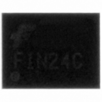
FIN24CGFX Fairchild Semiconductor, FIN24CGFX Datasheet - Page 6

FIN24CGFX
Manufacturer Part Number
FIN24CGFX
Description
IC SERIALIZER/DESERIAL 42-BGA
Manufacturer
Fairchild Semiconductor
Series
SerDes™r
Datasheet
1.FIN24CGFX.pdf
(25 pages)
Specifications of FIN24CGFX
Function
Serializer/Deserializer
Data Rate
520Mbps
Input Type
LVCMOS
Output Type
LVCMOS
Number Of Inputs
20
Number Of Outputs
20
Voltage - Supply
1.65 V ~ 3.6 V
Operating Temperature
-30°C ~ 70°C
Mounting Type
Surface Mount
Package / Case
42-BGA
Number Of Elements
1
Operating Temperature Classification
Commercial
Mounting
Surface Mount
Lead Free Status / RoHS Status
Lead free / RoHS Compliant
Other names
FIN24CGFX
FIN24CGFXTR
FIN24CGFXTR
Available stocks
Company
Part Number
Manufacturer
Quantity
Price
Company:
Part Number:
FIN24CGFX
Manufacturer:
FSC
Quantity:
6 506
Company:
Part Number:
FIN24CGFX
Manufacturer:
Fairchild Semiconductor
Quantity:
10 000
©2005 Fairchild Semiconductor Corporation
FIN24C Rev. 1.0.2
4-Bit Control Mode
When operating in 4-bit control mode, the master device
must be configured as MODE 2 (S2 = 1, S1 = 0) and the
slave device must be configured as MODE 1 (S2 = 0, S1
= 1). When operating in this mode, 24 data and control
bits can be sent from the master to the slave and 20 data
bits can be sent from the slave to the master. Unidirec-
tional control signals should be connected to DP[21:24].
2-Bit Control Mode
When operating in 2-bit control mode, both devices must
be configured in MODE 3 (S2 = S1 = “1”). In this mode,
22 bits can be sent in either direction. When operating in
a 2-bit control mode, serialized bits 21 and 22 appear on
outputs 23 and 24 of the deserializer.
6
Power-Down Mode: (Mode 0)
Mode 0 is used for powering down and resetting the
device. When both of the mode signals are driven to a
LOW state, the PLL and references are disabled, differ-
ential input buffers are shut off, differential output buffers
are placed into a HIGH-impedance state, LVCMOS out-
puts are placed into a HIGH-impedance state, LVCMOS
inputs are driven to a valid level internally, and all inter-
nal circuitry is reset. The loss of CKREF state is also
enabled to ensure that the PLL only powers up if there is
a valid CKREF signal.
In a typical application, the device only changes between
the power-down mode and the selected mode of opera-
tion. This allows for system-level power-down functional-
ity to be implemented via a single wire for a SerDes pair.
The S1 and S2 selection signals that have their operat-
ing mode driven to a “logic 0” should be hardwired to
GND. The S1 and S2 signals that have their operating
mode driven to a “logic 1” should be connected to a
system level power-down signal.
www.fairchildsemi.com


