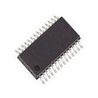
NB4N7132DTR2G ON Semiconductor, NB4N7132DTR2G Datasheet - Page 2

NB4N7132DTR2G
Manufacturer Part Number
NB4N7132DTR2G
Description
IC SRL LINK REPLICATR HP 28TSSOP
Manufacturer
ON Semiconductor
Type
Data Generator/Multiplexerr
Datasheet
1.NB4N7132DTR2G.pdf
(6 pages)
Specifications of NB4N7132DTR2G
Tx/rx Type
Ethernet
Delay Time
4.0ns
Voltage - Supply
3.135 V ~ 3.465 V
Current - Supply
125mA
Mounting Type
Surface Mount
Package / Case
28-TSSOP
Lead Free Status / RoHS Status
Lead free / RoHS Compliant
Capacitance - Input
-
Lead Free Status / Rohs Status
Compliant
Available stocks
Company
Part Number
Manufacturer
Quantity
Price
Part Number:
NB4N7132DTR2G
Manufacturer:
ON/安森美
Quantity:
20 000
Table 2. PIN DESCRIPTION
All VDD, VDDPx and GND Pins must be externally connected to appropriate power supply to guarantee proper operation.
OUT+
OUT-
MUX
4, 7, 14, 25
IN+
IN-
24, 23
18, 17
11, 12
28, 27
21, 20
10, 13
19, 22
1, 26
5, 6
Pin
15
16
2
8
3
9
Figure 2. Simplified Block Diagram
Table 1. OE, OUTPUT ENABLE FUNCTION
*Defaults to HIGH when left open
OUT0+, OUT0-
OUT1+, OUT1-
OUT+, OUT-
IN0+, IN0-
IN1+, IN1-
IN+, IN-
VDDP0
VDDP1
0
1
MUX1
MUX0
VDDP
Name
MUX
GND
VDD
OE0
OE1
OEx*
1
0
LVPECL Output
LVPECL Output
LVPECL Output
LVPECL Input
LVPECL Input
LVPECL Input
Power Supply
Power Supply
Power Supply
LVTTL Input
LVTTL Input
LVTTL Input
LVTTL Input
LVTTL Input
0
1
0
1
TYPICAL APPLICATIONS CIRCUIT
I/O
http://onsemi.com
Outputs Disabled OUTn+ = H, OUTn- = H
Non-inverted, Inverted, Differential Data Inputs internally biased to
Approximately 1.2 V.
Non-inverted, Inverted Differential Outputs.
OE0/OE1 enables OUT0/OUT1 when HIGH. When LOW, OUTx are
powered down and both OUT+ and OUT- float HIGH.
Selects Source for OUT, Selects Either IN0 (LOW) or IN1 (HIGH); defaults
HIGH when left open.
Selects Source for OUT1. Selects Either IN (HIGH) or IN0 (LOW); defaults
HIGH when left open.
Selects Source for OUT0. Selects either IN (LOW) or IN1 (HIGH); defaults
HIGH when left open.
3.3 V Positive Supply Voltage for Digital Logic.
3.3 V supply for LVPECL output drivers. VDDP is for OUT, VDDP0 is for
OUT0, and VDDP1 is for OUT1.
Negative Supply Voltage, Connected to Ground
NB4N7132
IN0+
IN0-
OE0
OUT0+
OUT0-
MUX0
IN1+
IN1-
OE1
OUT1+
OUT1-
MUX1
2
Outputs Enabled
Function
VDDP0
VDDP
VDDP
OUT+
OUT-
MUX
GND
GND
GND
VDD
OE0
OE1
IN+
IN-
Figure 3. Pin Diagram for TSSOP-28
10
12
13
14
11
1
2
3
4
5
6
7
8
9
Description
NB4N7132
28
27
26
25
24
23
22
21
20
19
18
17
16
15
OUT0+
OUT0-
VDDP0
GND
IN0+
IN0-
VDDP1
OUT1+
OUT1-
VDDP1
IN1+
IN1-
MUX0
MUX1


