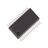
NB4N7132DTR2G ON Semiconductor, NB4N7132DTR2G Datasheet - Page 4

NB4N7132DTR2G
Manufacturer Part Number
NB4N7132DTR2G
Description
IC SRL LINK REPLICATR HP 28TSSOP
Manufacturer
ON Semiconductor
Type
Data Generator/Multiplexerr
Datasheet
1.NB4N7132DTR2G.pdf
(6 pages)
Specifications of NB4N7132DTR2G
Tx/rx Type
Ethernet
Delay Time
4.0ns
Voltage - Supply
3.135 V ~ 3.465 V
Current - Supply
125mA
Mounting Type
Surface Mount
Package / Case
28-TSSOP
Lead Free Status / RoHS Status
Lead free / RoHS Compliant
Capacitance - Input
-
Lead Free Status / Rohs Status
Compliant
Available stocks
Company
Part Number
Manufacturer
Quantity
Price
Part Number:
NB4N7132DTR2G
Manufacturer:
ON/安森美
Quantity:
20 000
NOTE: Device will meet the specifications after thermal equilibrium has been established when mounted in a test socket or printed circuit
NOTE: Device will meet the specifications after thermal equilibrium has been established when mounted in a test socket or printed circuit
3. Measured 20% to 80%
Table 5. DC CHARACTERISTICS
LVCMOS/LVTTL INPUTS
Table 6. AC CHARACTERISTICS
V
I
P
DV
DV
DV
V
V
I
I
f
tr/tf
t
T
Symbol
Symbol
DD
IH
IL
IN / OUT
PD
DJ
DD
D
IH
IL
IN
OUT50
OUT75
board with maintained transverse airflow greater than 500 lfpm. Electrical parameters are guaranteed only over the declared
operating temperature range. Functional operation of the device exceeding these conditions is not implied. Device specification limit
values are applied individually under normal operating conditions and not valid simultaneously.
OUT0+/-
OUT1+/-
OUT+/-
IN0+/-
IN1+/-
IN+/-
Power Supply Voltage, 3.30 V $5%
Power Supply Current (Outputs open)
Power Dissipation; Outputs Open; V
Receiver Differential Voltage Amplitude; (IN, IN0, IN1), AC-Coupled,
Internally Biased to 1.2 V;
Output Differential Voltage Swing, peak-peak; (OUT, OUT0, OUT1)
Outputs loaded / terminated with 50 W to V
Output Differential Voltage Swing, peak-peak; (OUT, OUT0, OUT1)
Outputs loaded / terminated with 75 W to V
Input HIGH Voltage, TTL
Input LOW Voltage, TTL
Input HIGH Current, TTL; V
Input LOW Current, TTL; V
Input / Output Frequency Range
Output rise and Fall Times (Note 3)
Propagation Delay, IN to OUT
Deterministic Jitter Added to Serial Input Up to 1.5 Gb/s;
K28.5$ Pattern
Differential Measurement - (V
Differential Measurement - (V
Characteristic
IN
V
V
IN
t
Characteristic
pd
Differential Measurement - (V
DD
DD
= 0.5 V
= 2.4 V
= 3.30 V $5%, GND = 0 V; T
= 3.3 V $5%, GND = 0 V -40°C to +85°C
DD
Figure 4. Timing Waveforms
= V
DD
DD
DDmax
http://onsemi.com
– 2.0 V
– 2.0 V
NB4N7132
OUTn+
OUTn+
4
INn+
- V
- V
A
- V
= -40°C to +85°C
OUTn-
OUTn-
t
pd
INn-
)
)
)
Min
1.0
1000
1200
-100
3.14
Min
300
2.0
0
t
J
0.375
Typ
140
Typ
105
Max
175
1.5
4.0
40
V
DD
2600
2200
2200
Max
3.47
125
450
100
0.8
+ 0.5
ps pk-pk
Gb/s
Unit
ps
ns
Unit
mW
mA
mV
mV
mV
mA
mA
V
V
V


