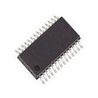
NB4N7132DTR2G ON Semiconductor, NB4N7132DTR2G Datasheet - Page 5

NB4N7132DTR2G
Manufacturer Part Number
NB4N7132DTR2G
Description
IC SRL LINK REPLICATR HP 28TSSOP
Manufacturer
ON Semiconductor
Type
Data Generator/Multiplexerr
Datasheet
1.NB4N7132DTR2G.pdf
(6 pages)
Specifications of NB4N7132DTR2G
Tx/rx Type
Ethernet
Delay Time
4.0ns
Voltage - Supply
3.135 V ~ 3.465 V
Current - Supply
125mA
Mounting Type
Surface Mount
Package / Case
28-TSSOP
Lead Free Status / RoHS Status
Lead free / RoHS Compliant
Capacitance - Input
-
Lead Free Status / Rohs Status
Compliant
Available stocks
Company
Part Number
Manufacturer
Quantity
Price
Part Number:
NB4N7132DTR2G
Manufacturer:
ON/安森美
Quantity:
20 000
IN+/IN- Input Functionality
a typical application, the differential inputs are
capacitor-coupled and will swing symmetrically above and
below 1.2 V, preserving a 50% duty cycle to the outputs.
differential input allowing for LVPECL, CML, LVDS, and
HSTL input levels.
OUT+ / OUT- Outputs
designed to drive differential transmission lines with
nominally 50 W or 75 W characteristic impedance. These
differential output buffers utilize positive emitter coupled
logic (PECL) architecture, but they do not require DC output
load resistors, and will operate properly with or without the
resistors.
†For information on tape and reel specifications, including part orientation and tape sizes, please refer to our Tape and Reel Packaging
ORDERING INFORMATION
Specifications Brochure, BRD8011/D.
NB4N7132DTG
NB4N7132DTR2G
The differential inputs are internally biased to Y1.2 V. In
With this technique, the NB4N7132 will accept any
The OUT+ and OUT- outputs of the NB4N7132 are
SerDes
RX+
RX-
TX+
TX-
Device
R
R
RT
0.01mF
0.01mF
0.01mF
0.01mF
RT
Figure 5. NB4N7132 Application Interface Example
Resource Reference of Application Notes
AND8002
AND8009
“R” is 150 W for both 100 W differential or 150 W differential traces.
“RT” matches the differential impedance of the link.
I+
I-
O+
O-
TSSOP-28
TSSOP-28
NB4N7132
(Pb-Free)
(Pb-Free)
Package
O1+
O1-
I1+
I1-
-
-
http://onsemi.com
Marking and Date Codes
ECLinPS Plus Spice I/O Model Kit
NB4N7132
RT
0.01mF
0.01mF
0.01mF
0.01mF
5
OEx Output Enable
OE1, that work by powering down the output buffer and
associated driving circuitry. Using this approach results in
both differential outputs going HIGH, and a reduction in I
current of approx. 29 mA for each disabled output pair.
When OEx is LOW, outputs are disabled, OUTx+ and
OUTx- are set HIGH.
Power Supply Bypass information
the device. The NB4N7132 provides separate power supply
pins for the digital circuitry (V
(VDDPn). Placing a bypass capacitor of 0.01 mF to 0.1 mF
on each VDD pin will help ensure a noise free V
supply. The purpose of this design technique is to try and
isolate the high switching noise of the digital outputs from
the relatively sensitive digital core logic.
The NB4N7132 incorporates output enable pins, OE0 and
A clean power supply will optimize the performance of
RT
I1+
I1-
O1+
O1-
NB4N7132
O+
O-
2500 / Tape & Reel
I+
I-
50 Units / Rail
Shipping
0.01mF
0.01mF
RT
†
0.01mF
0.01mF
DD
) and LVPECL outputs
RT
R
R
RX+
RX-
TX+
TX-
SerDes
DD
power
DD


