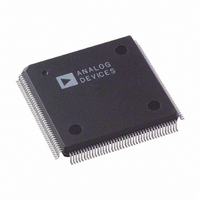
AD9887AKSZ-170 Analog Devices Inc, AD9887AKSZ-170 Datasheet - Page 28

AD9887AKSZ-170
Manufacturer Part Number
AD9887AKSZ-170
Description
IC INTRFACE ANALOG/DVI 160-MQFP
Manufacturer
Analog Devices Inc
Specifications of AD9887AKSZ-170
Applications
Graphic Cards, VGA Interfaces
Interface
Analog and Digital
Voltage - Supply
3.15 V ~ 3.45 V
Package / Case
160-MQFP, 160-PQFP
Mounting Type
Surface Mount
Supply Voltage Range
3.15V To 3.45V, 2.2V To 3.45V
Operating Temperature Range
0°C To +70°C
Digital Ic Case Style
MQFP
No. Of Pins
160
Msl
MSL 3 - 168 Hours
Termination Type
SMD
Rohs Compliant
Yes
Filter Terminals
SMD
Bandwidth
170MHz
Lead Free Status / RoHS Status
Lead free / RoHS Compliant
Available stocks
Company
Part Number
Manufacturer
Quantity
Price
Company:
Part Number:
AD9887AKSZ-170
Manufacturer:
ADI
Quantity:
437
Company:
Part Number:
AD9887AKSZ-170
Manufacturer:
Analog Devices Inc
Quantity:
10 000
Part Number:
AD9887AKSZ-170
Manufacturer:
AD
Quantity:
20 000
AD9887A
SCAN FUNCTION
The scan function is intended as a pseudo JTAG function for the
manufacturing test of the board. The ordinary operation of the
AD9887A is disabled during scanning. To enable the scan function,
set Register 0x14, Bit 2, to 1. To scan data to all 48 digital outputs,
apply 48 serial bits of data and 48 clock cycles (typically 5 MHz,
maximum of 20 MHz) to the SCAN
respectively. The data is shifted in upon the rising edge of SCAN
The first serial bit shifted in appears at the RED A<7> output after
one clock cycle.
BLUE B<0>
RED A<7>
SCAN
SCAN
SCAN
OUT
CLK
IN
BIT 1
IN
X
SCAN
and SCAN
SCAN
BIT 1
X
CLK
IN
BIT 2
X
CLK
BIT 2
X
pins,
t
Figure 31. Scan Set-up and Hold Times
SU
BIT 3
= 3ns
X
BIT 3
Figure 30. Scan Timing
Rev. B | Page 28 of 52
X
CLK
.
BIT 46
t
X
HOLD
BIT 47
= 0ns
After the next clock cycle, the first bit is shifted to RED A<6> and
the next bit appears at RED A<7>. After 48 clock cycles, the first
bit is shifted to the BLUE B<0> output and the 48th bit appears
at the RED A<7> output. If SCAN
the data continues to be shifted from RED A<7> to BLUE B<0>
and comes out of the SCAN
edge of SCAN
of 3 ns should be more than adequate; no hold time (t
required (0 ns). This is illustrated in Figure 31.
X
BIT 47
X
BIT 48
X
BIT 48
BIT 1
CLK
. This is illustrated in Figure 30. A setup time (t
BIT 1
X
BIT 2
X
OUT
BIT 2
pin as serial data upon the falling
CLK
continues after 48 cycles,
HOLD
) is
SU
)


