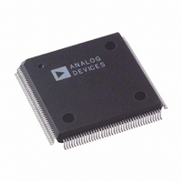
AD9887AKSZ-170 Analog Devices Inc, AD9887AKSZ-170 Datasheet - Page 29

AD9887AKSZ-170
Manufacturer Part Number
AD9887AKSZ-170
Description
IC INTRFACE ANALOG/DVI 160-MQFP
Manufacturer
Analog Devices Inc
Specifications of AD9887AKSZ-170
Applications
Graphic Cards, VGA Interfaces
Interface
Analog and Digital
Voltage - Supply
3.15 V ~ 3.45 V
Package / Case
160-MQFP, 160-PQFP
Mounting Type
Surface Mount
Supply Voltage Range
3.15V To 3.45V, 2.2V To 3.45V
Operating Temperature Range
0°C To +70°C
Digital Ic Case Style
MQFP
No. Of Pins
160
Msl
MSL 3 - 168 Hours
Termination Type
SMD
Rohs Compliant
Yes
Filter Terminals
SMD
Bandwidth
170MHz
Lead Free Status / RoHS Status
Lead free / RoHS Compliant
Available stocks
Company
Part Number
Manufacturer
Quantity
Price
Company:
Part Number:
AD9887AKSZ-170
Manufacturer:
ADI
Quantity:
437
Company:
Part Number:
AD9887AKSZ-170
Manufacturer:
Analog Devices Inc
Quantity:
10 000
Part Number:
AD9887AKSZ-170
Manufacturer:
AD
Quantity:
20 000
THEORY OF OPERATION—DIGITAL INTERFACE
CAPTURING ENCODED DATA
The first step in recovering encoded data is to capture the raw data.
To accomplish this, the AD9887A uses a high speed, phase-locked
loop (PLL) to generate clocks capable of oversampling the data
at the correct frequencies. The data capture circuitry continuously
monitors the incoming data during horizontal and vertical
blanking periods (when DE is low) and independently selects
the best sampling phase for each data channel. The phase infor-
mation is stored and used until the next blanking period (one
video line).
DATA FRAMES
The digital interface data is captured in groups, called data
frames, of 10 bits each. During the active data period, each
frame is made up of nine encoded video data bits and one dc-
balancing bit. The data capture block receives this data serially,
but outputs each frame in parallel, 10-bit words.
SPECIAL CHARACTERS
During periods of horizontal or vertical blanking (when DE is
low), the digital transmitter transmits special characters that are
used to set the video frame boundaries and the phase recovery
loop for each channel. There are four special characters that can
be received. They are used to identify the top, bottom, left side,
and right side of each video frame. The data receiver can differ-
entiate these special characters from active data, because the
special characters have a different number of transitions per
data frame.
CHANNEL RESYNCHRONIZATION
The purpose of the channel resynchronization block is to
resynchronize the three data channels to a single internal data
clock. Even if all three data channels are on different phases of
the PLL clock (0°, 120°, and 240°), this block can resynchronize
the channels from a worst-case skew of one full input period
(8.93 ns at 170 MHz).
DATA DECODER
The data decoder receives frames of data and sync signals from
the data capture block in 10-bit, parallel words and decodes
them into groups of eight RGB/YUV bits, two control bits, and
a data enable (DE) bit.
Rev. B | Page 29 of 52
HDCP
The AD9887A contains circuitry necessary for decrypting
a high-bandwidth digital content protection (HDCP) encoded
DVI video stream. A typical HDCP implementation is shown in
Figure 32. Several features of the AD9887A make decryption
possible and ease the implementation of HDCP.
The basic components of HDCP are included in the AD9887A.
A slave serial bus connects to the DDC clock and the DDC data
pins on the DVI connector to allow the HDCP-enabled DVI
transmitter to coordinate the HDCP algorithm with the
AD9887A. A second serial port (MDA/MCL) allows the
AD9887A to read the HDCP keys and key selection vector
(KSV) stored in an external serial EEPROM. When transmitting
encrypted video, the DVI transmitter enables HDCP through
the DDC port.
The AD9887A then decodes the DVI stream using information
provided by the transmitter, HDCP keys, and KSV. The AD9887A
allows the MDA and MCL pins to be three-state, using the
MDA/MCL three-state bit (Register 0x1B, Bit 7) in the
configuration registers. The three-state feature allows the EEPROM
to be programmed in-circuit. The MDA/MCL port must be
three-state before attempting to program the EEPROM using an
external master. The keys are stored in an I
serial EEPROM of at least 512 bytes. The EEPROM should have
a device address of 0xA0.
Proprietary software licensed from Analog Devices, Inc. encrypts
the keys and creates properly formatted EEPROM images for
use in a production environment. Encrypting the keys helps
maintain the confidentiality of the HDCP keys, as required by
the HDCP v1.0 specification. The AD9887A includes hardware
for decrypting the keys in the external EEPROM.
ADI provides a royalty-free license for the proprietary software
needed by customers to encrypt the keys between the AD9887A
and the EEPROM only after customers provide evidence of a
completed HDCP Adopter’s License Agreement and sign the Analog
Devices Software License Agreement. The Adopter’s License
Agreement is maintained by Digital Content Protection, LLC
and can be downloaded from www.digital-cp.com. To obtain the
Analog Devices Software License Agreement, contact the Display
Electronics Product Line directly by sending an email to
flatpanel_apps@analog.com.
2
C®-compatible 3.3 V
AD9887A


