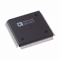
AD9887AKSZ-170 Analog Devices Inc, AD9887AKSZ-170 Datasheet - Page 36

AD9887AKSZ-170
Manufacturer Part Number
AD9887AKSZ-170
Description
IC INTRFACE ANALOG/DVI 160-MQFP
Manufacturer
Analog Devices Inc
Specifications of AD9887AKSZ-170
Applications
Graphic Cards, VGA Interfaces
Interface
Analog and Digital
Voltage - Supply
3.15 V ~ 3.45 V
Package / Case
160-MQFP, 160-PQFP
Mounting Type
Surface Mount
Supply Voltage Range
3.15V To 3.45V, 2.2V To 3.45V
Operating Temperature Range
0°C To +70°C
Digital Ic Case Style
MQFP
No. Of Pins
160
Msl
MSL 3 - 168 Hours
Termination Type
SMD
Rohs Compliant
Yes
Filter Terminals
SMD
Bandwidth
170MHz
Lead Free Status / RoHS Status
Lead free / RoHS Compliant
Available stocks
Company
Part Number
Manufacturer
Quantity
Price
Company:
Part Number:
AD9887AKSZ-170
Manufacturer:
ADI
Quantity:
437
Company:
Part Number:
AD9887AKSZ-170
Manufacturer:
Analog Devices Inc
Quantity:
10 000
Part Number:
AD9887AKSZ-170
Manufacturer:
AD
Quantity:
20 000
AD9887A
0x03 4–2
Table 11. Charge-Pump Currents
CURRENT
000
001
010
011
100
101
110
111
0x04 7:3
Clamp Timing
0x05 7:0
0x06 7:0
Three bits that establish the current driving the loop
filter in the clock generator.
See Table 7 for the recommended CURRENT settings.
The power-up default value is CURRENT = 001.
A 5-bit value that adjusts the sampling phase in 32 steps
across one pixel period. Each step represents an 11.2°
shift in sampling phase.
The power-up default value is 16.
An 8-bit register that sets the position of the internally
generated clamp.
When EXTCLMP = 0, a clamp signal is generated
internally at a position established by the clamp
placement for a duration set by the clamp duration.
Clamping is started [clamp placement] pixel periods
after the trailing edge of Hsync. The clamp placement
can be programmed to any value between 1 and 255.
A value of 0 is not supported.
The clamp should be placed during a time when the
input signal presents a stable black-level reference,
usually during a period between Hsync and the image
called the back porch. When EXTCLMP = 1, this
register is ignored.
An 8-bit register that sets the duration of the internally
generated clamp.
When EXTCLMP = 0, a clamp signal is generated
internally at a position established by the clamp
placement for a duration set by the clamp duration.
Clamping is started [clamp placement] pixel periods
after the trailing edge of Hsync and continues for [clamp
duration] pixel periods. The clamp duration can be
programmed to a value between 1 and 255. A value of 0
is not supported.
CURRENT Charge-Pump Current
Clock Phase Adjust
Clamp Placement
Clamp Duration
50
100
150
250
350
500
750
1500
Current (μA)
Rev. B | Page 36 of 52
Hsync Pulse Width
0x07 7:0
Input Gain
0x08 7:0
0x09 7:0
0x0A 7:0
Input Offset
0x0B 7:1
For the best results, the clamp duration should be set to
include the majority of the black reference signal time
that follows the Hsync signal trailing edge. Insufficient
clamping time can produce brightness changes at the top
of the screen and can cause slow recovery from large
changes in the average picture level (APL) or brightness.
When EXTCLMP = 1, this register is ignored.
An 8-bit register that sets the duration of the Hsync
output pulse.
The leading edge of the Hsync output is triggered by the
internally generated, phase-adjusted PLL feedback clock.
The AD9887A counts the number of pixel clock cycles
set in this register. This triggers the trailing edge of the
Hsync output, which is also phase adjusted.
An 8-bit word that sets the gain of the red channel.
The AD9887A can accommodate input signals with a
full-scale range between 0.5 V and 1.5 V p-p. Setting
REDGAIN to 255 corresponds to an input range of
1.0 V. A REDGAIN of 0 establishes an input range of
0.5 V. Note that increasing REDGAIN results in the
picture having less contrast because the input signal uses
fewer of the available converter codes (see Figure 6).
An 8-bit word that sets the gain of the green channel. See
REDGAIN (0x08).
An 8-bit word that sets the gain of the blue channel. See
REDGAIN (0x08).
A 7-bit offset binary word that sets the dc offset of the
red channel (REDOFST). An offset adjustment of 1 LSB
equals approximately 1 LSB change in the ADC offset.
Therefore, the absolute magnitude of the offset adjustment
scales as the gain of the channel changes. A nominal setting
of 63 results in the channel nominally clamping to Code 00
during the back porch clamping interval. An offset setting
of 127 results in the channel clamping to Code 63 of the
ADC. An offset setting of 0 clamps to Code −63 (off the
bottom of the range). Increasing the value of red offset
decreases the brightness of the channel.
Red Channel Gain Adjust (REDGAIN)
Green Channel Gain Adjust (GREENGAIN)
Blue Channel Gain Adjust (BLUEGAIN)
Red Channel Offset Adjust (REDOFST)
Hsync Output Pulse Width


