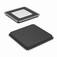
ISL54105CRZ Intersil, ISL54105CRZ Datasheet

ISL54105CRZ
Specifications of ISL54105CRZ
Available stocks
Related parts for ISL54105CRZ
ISL54105CRZ Summary of contents
Page 1
... PART NUMBER TEMP. RANGE (°C) ISL54105CRZ NOTE: These Intersil Pb-free plastic packaged products employ special Pb-free material sets, molding compounds/die attach materials, and 100% matte tin plate plus anneal (e3 termination finish, which is RoHS compliant and compatible with both SnPb and Pb-free soldering operations). Intersil Pb-free products are MSL classified at Pb-free peak reflow temperatures that meet or exceed the Pb-free requirements of IPC/JEDEC J STD-020 ...
Page 2
... QFN Package Maximum Biased Junction Temperature . . . . . . . . . . . . . . . . +125°C Storage Temperature . . . . . . . . . . . . . . . . . . . . . . . .-65°C to +150°C Pb-Free Reflow Profile .see link below http://www.intersil.com/pbfree/Pb-FreeReflow.asp Recommended Operating Conditions Temperature . . . . . . . . . . . . . . . . . . . . . . . . . . . . . . . . 0°C to +70°C Supply Voltage 3.3V, pixel rate = 165MHz +25°C, RES_TERM = 1kΩ, RES_BIAS = 3.16kΩ, ...
Page 3
Electrical Specifications Specifications apply for V TMDS output load = 50Ω, TMDS output termination voltage V SYMBOL PARAMETER DIGITAL OUTPUT CHARACTERISTICS V Output HIGH Voltage 8mA Output LOW Voltage -8mA OL O POWER ...
Page 4
ISL54105 Pin Configuration RES_TERM RES_BIAS RXC- 12 RXC ...
Page 5
Pin Descriptions SYMBOL RX0-, RX0+, RX1-, RX1+, RX2-, RX2+ TMDS Inputs. Incoming TMDS data signals. RXC-, RXC+ TMDS Inputs. Incoming TMDS clock signals. TX0-, TX0+, TX1-, TX1+, TX1-, TX1+ TMDS Outputs. TMDS output data for selected channel. TXC-, TXC+ SCL ...
Page 6
Register Listing ADDRESS REGISTER (DEFAULT VALUE) 0x00 Device ID (read only) 0x01 Channel Activity Detect (read only) 0x02 Channel Selection (0x0C) 0x03 Input Control (0x12) Recommended default: 0x63 6 ISL54105 BIT(S) FUNCTION NAME 3:0 Device Revision 1 = initial silicon, ...
Page 7
Register Listing (Continued) ADDRESS REGISTER (DEFAULT VALUE) 0x04 Termination Control (0x00) 0x05 Output Options (0x00) 0x06 Data Output Drive (0x00) 0x07 Reserved (0xCC) 0x08 Equalization (0xCC) 0x09 Test Pattern Generator (0x00) 7 ISL54105 BIT(S) FUNCTION NAME 1:0 Reserved Set to ...
Page 8
Register Listing (Continued) ADDRESS REGISTER (DEFAULT VALUE) 0x0A PRBS7 Error Counter Link 0 (read only) 0x0B PRBS7 Error Counter Link 1 (read only) 0x0C PRBS7 Error Counter Link 2 (read only) 0x10 PLL Bandwidth (0x10) Recommended default: 0x12 8 ISL54105 ...
Page 9
Application Information The ISL54105 is a TMDS regenerator, locking to the incoming DVI or HDMI signal with triple Clock Data Recovery units (CDRs) and a Phase Locked Loop (PLL). The PLL generates a low jitter pixel clock from the incoming ...
Page 10
Next, a 15m DualLink DVI cable was attached and terminated into a female TPA2 adapter and the eye captured in Figure 4. FIGURE 4. CHROMA EYE DIAGRAM AFTER 15m CABLE The eye is not meeting the minimum requirements of either ...
Page 11
... 0.1μF ISL54105 FIGURE 9. SCHOTTKY DIODE MODIFICATION Intersil is currently sampling the ISL54105A, which is fully compliant with Test 7-3 when applied using the circuit shown in Figure 9. The ISL54105A is 100% drop-in and backwards compatible with the ISL54105. 11 ISL54105 Using the ISL54105A in a layout designed for the ISL54105 (Figure 8) will result in the same behavior as the original version ...
Page 12
The FIFO’s quantization (worst case) increases the total skew to 4.0 bits. Bit 5 Bit 4 Bit 3 Bit 2 Bit 1 Bit 0 INPUT SKEW (2.3 bits/1.4ns Bit 7 Bit ...
Page 13
VIA TO POWER PLANE + V C BYPASS GND VIAS TO GND EQUIVALENT CIRCUIT POWER PLANE R VIA R R TRACE TRACE + V C BYPASS GROUND PLANE FIGURE 13. OPTIMAL (“T”) BYPASS CAPACITOR LAYOUT ISL54105 Serial Communication Overview The ...
Page 14
SCL FROM HOST DATA OUTPUT FROM TRANSMITTER DATA OUTPUT FROM RECEIVER START FIGURE 15. ACKNOWLEDGE RESPONSE FROM RECEIVER SCL SDA FIGURE 16. VALID DATA CHANGES ON THE SDA BUS START Command ISL54105 Serial Bus ADDR6 ADDR5 ADDR4 ADDR3 ADDR2 A7 ...
Page 15
... Accordingly, the reader is cautioned to verify that data sheets are current before placing orders. Information furnished by Intersil is believed to be accurate and reliable. However, no responsibility is assumed by Intersil or its subsidiaries for its use; nor for any infringements of patents or other rights of third parties which may result from its use ...
Page 16
Package Outline Drawing L72.10x10B 72 LEAD QUAD FLAT NO-LEAD PLASTIC PACKAGE (PUNCH QFN) Rev 0, 5/07 10.00 9. PIN 1 INDEX AREA (4X) 0.15 TOP VIEW PACKAGE OUTLINE 4.70 10.00 TYPICAL RECOMMENDED LAND PATTERN 11° ±1° ALL ...


