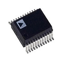
AD7011ARS Analog Devices Inc, AD7011ARS Datasheet

AD7011ARS
Specifications of AD7011ARS
Available stocks
Related parts for AD7011ARS
AD7011ARS Summary of contents
Page 1
FEATURES Single +5 V Supply On-Chip /4 DQPSK Modulator Modulator Bypass Analog Mode Root-Raised Cosine Tx Filters, Two 10-Bit D/A Converters 4th Order Reconstruction Filters Differential Analog Outputs On-Chip Ramp Up/Down Power Control On-Chip Tx Offset Calibration Dual Mode ...
Page 2
... The user should ensure that binary codes greater than or less than the maximum or minimum are not loaded into the DACs. 5 Measured while the digital inputs to the transmit interface are static and equal Specifications subject to change without notice 10%; Test = AGND = DGND = 0 V; Digital Mode All specifications are T DD AD7011ARS REF REF +V /2 REF 0.875 7. ...
Page 3
AA MASTER CLOCK TIMING otherwise noted.) Parameter Limit 300 1 t 100 2 t 100 MCLK Figure 2. Master Clock (MCLK) Timing REV. B ITx/QTx 20pF 20k AD7011 20k ITx / ...
Page 4
AD7011 TRANSMIT SECTION TIMING Parameter Limit – + – 4097t + – ...
Page 5
AA ANALOG MODE TIMING otherwise noted.) Parameter Limit – + 15t 1 t 16t MCLK t 20 FRAME ...
Page 6
... Although this device features proprietary ESD protection circuitry, permanent damage may occur on devices subjected to high energy electrostatic discharges. Therefore, proper ESD precautions are recommended to avoid performance degradation or loss of functionality. Model Temperature Range AD7011ARS – +85 C Junction Temperature . . . . . . . . . . . . . . . . . . . . . . . . +150 C SSOP Thermal Impedance . . . . . . . . . . . . . . . . +122 C/W ...
Page 7
SSOP Pin Number Mnemonic Function POWER SUPPLY 19 V Positive power supply for analog section Positive power supply for digital section. DD 14, 18, 23 AGND Analog ground for transmit section. 6 DGND Digital ground for transmit ...
Page 8
AD7011 TERMINOLOGY Error Vector Magnitude This is a measure of the rms error vector introduced by the AD7011 where signal error vector is defined as the rms devia- tion of a transmitted symbol from its ideal position when filtered by ...
Page 9
CIRCUIT DESCRIPTION TRANSMIT SECTION The transmit section of the AD7011 generates /4 DQPSK I and Q waveforms in accordance with TIA specification. This is accomplished by a digital /4 DQPSK modulator, which includes the root-raised cosine filters ( = 0.35), ...
Page 10
AD7011 BIN TxCLK TxDATA BOUT (ITx–ITx), (QTx–QTx) SYMBOL PHASE MAX EFFECT As Figure 12 illustrates, the ramp-down envelope reaches zero after three symbols, hence the fourth symbol does not actually get transmitted. ...
Page 11
FREQUENCY – kHz Figure 13. Reconstruction Filter Frequency Response for the I and Q DACs, MCLK = 2.56 MHz 1.2 1.2 0.8 0.8 0.4 0 –0.4 ...
Page 12
AD7011 PIN 1 0.008 (0.203) 0.002 (0.050) OUTLINE DIMENSIONS Dimensions shown in inches and (mm). 24-Lead SSOP (RS-24 0.212 (5.38) 0.205 (5.207) 0.311 (7.9) 0.301 (7.64 0.07 (1.78) 0.328 (8.33) 0.318 (8.08) 0.066 (1.67) 8° 0° ...


