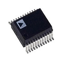
AD7011ARS Analog Devices Inc, AD7011ARS Datasheet - Page 7

AD7011ARS
Manufacturer Part Number
AD7011ARS
Description
Manufacturer
Analog Devices Inc
Datasheet
1.AD7011ARS.pdf
(12 pages)
Specifications of AD7011ARS
Device Type
Modulator
Modulation Type
Quadrature
Pin Count
24
Package Type
SSOP
Lead Free Status / Rohs Status
Not Compliant
Available stocks
Company
Part Number
Manufacturer
Quantity
Price
Part Number:
AD7011ARS
Manufacturer:
ADI/亚德诺
Quantity:
20 000
Part Number:
AD7011ARSZ
Manufacturer:
ADI/亚德诺
Quantity:
20 000
REV. B
SSOP Pin
Number
POWER SUPPLY
19
5
14, 18, 23
6
ANALOG SIGNAL AND REFERENCE
13
16, 17
21, 20
TRANSMIT INTERFACE AND CONTROL
7
3
4
2
24
1
12
9, 11
8, 10, 15, 22 NC
Mnemonic
V
V
AGND
DGND
BYPASS
ITx, ITx
QTx, QTx
MCLK
TxCLK
(FRAME)
TxDATA
(IDATA)
BIN (QDATA) This is a dual function digital input. When operating in Mode 0 (TIA Digital mode), this input is used to ini-
BOUT
POWER
READY
MODE1,
MODE2
AA
DD
Function
Positive power supply for analog section.
Positive power supply for digital section.
Analog ground for transmit section.
Digital ground for transmit section.
Reference decoupling output. A decoupling capacitor should be connected between this pin and AGND.
Differential analog outputs for the I channel, representing true and complementary outputs of the I
waveform.
Differential analog outputs for the Q channel, representing true and complementary outputs of the Q
waveform.
Master clock, digital input. When operating in Mode 0 (TIA Digital mode), this pin should be driven by a
3.1104 MHz CMOS compatible clock source in digital mode and by 2.56 MHz CMOS compatible clock
source for analog mode.
This is a dual function digital input/output. When operating in Mode 0 (TIA Digital mode), this pin is
configured as a digital output, transmit clock. This may be used to clock in transmit data at 48.6 kHz. When
operating in Mode 1 (analog mode), this pin is configured as a digital input, FRAME. This is used to frame
the clocking in of 16-bit words when bypassing the /4 DQPSK modulator and directly loading the I and Q
10-bit DACs.
This is a dual function digital input. When operating in Mode 0 (TIA Digital mode), this pin is used to
clock in transmit data on the falling edge of TxCLK at a rate of 48.6 kHz. When operating in Mode 1
(Analog mode), I data is clocked in on the rising edge of MCLK. This data bypasses the /4 DQPSK modu-
lator and is loaded into the 10-bit I DAC.
tiate the ramping up (BIN high) or down (BIN low) of the I and Q waveforms. When operating in Mode 1
(Analog mode), Q data is clocked in on the rising edge of MCLK. This data bypasses the /4 DQPSK modu-
lator and is loaded into the 10-bit Q DAC.
Burst Out, digital output. This is the BIN input delayed by the pipeline delay, both digital and analog, of the
AD7011. This can be used to turn on and off the RF amplifiers in synchronization with the I and Q waveforms.
Transmit sleep mode, digital input. When this goes low, the AD7011 goes into sleep mode, drawing minimal
current. When this pin goes high, the AD7011 is brought out of sleep mode and initiates a self-calibration
routine to eliminate the offset between ITx & ITx and the offset between QTx & QTx.
Transmit ready, digital output. This output goes high once the self-calibration routine is complete.
Mode control, digital inputs. These are used to enter the AD7011 into three different operating modes,
see Table I.
No Connects. These pins are no connects and should not be used as routes for other circuit signals.
PIN FUNCTION DESCRIPTION
–7–
AD7011


