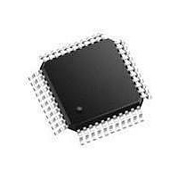
UDA1384H NXP Semiconductors, UDA1384H Datasheet - Page 22

UDA1384H
Manufacturer Part Number
UDA1384H
Description
Encoders, Decoders, Multiplexers & Demultiplexers LO CST MULTICH CODEC
Manufacturer
NXP Semiconductors
Datasheet
1.UDA1384H.pdf
(55 pages)
Specifications of UDA1384H
Maximum Operating Temperature
+ 85 C
Package / Case
SOT-307
Minimum Operating Temperature
- 20 C
Mounting Style
SMD/SMT
Lead Free Status / Rohs Status
Details
Other names
UDA1384H/N1,557
Available stocks
Company
Part Number
Manufacturer
Quantity
Price
Company:
Part Number:
UDA1384H/N1,518
Manufacturer:
NXP Semiconductors
Quantity:
10 000
Company:
Part Number:
UDA1384H/N1,557
Manufacturer:
NXP Semiconductors
Quantity:
10 000
Philips Semiconductors
9397 750 14366
Product data sheet
10.11 Write cycle
10.12 Read cycle
The write cycle is used to write groups of two bytes to the internal registers for the
settings. It is also possible to read the registers for the device status information.
The I
write the data to the internal registers. The device and register addresses are one byte
each, the setting data is always a pair of two bytes.
The format of the write cycle is as follows:
Table 18:
[1]
The read cycle is used to read the data values from the internal registers. The I
configuration for a read cycle is shown in
The format of the read cycle is as follows:
S 0011 000 0
1. The microcontroller starts with a start condition (S).
2. The first byte (8 bits) contains the device address ‘0011 000’ and a logic 0 (write) for
3. This is followed by an acknowledge (A) from the UDA1384.
4. After this the microcontroller writes the 8-bit register address (ADDR) where the
5. The UDA1384 acknowledges this register address (A).
6. The microcontroller sends 2 bytes data with the Most Significant (MS) byte first and
7. If repeated groups of 2 bytes data are transmitted, then the register address is auto
8. Finally, the UDA1384 frees the I
1. The microcontroller starts with a start condition (S).
2. The first byte (8 bits) contains the device address ‘0011 000’ and a logic 0 (write) for
3. This is followed by an acknowledge (A) from the UDA1384.
4. After this the microcontroller writes the 8-bit register address (ADDR) where the
5. The UDA1384 acknowledges this register address.
6. Then the microcontroller generates a repeated start (Sr).
Device
address
A = acknowledge from UDA1384
the R/W bit.
writing of the register content of the UDA1384 must start.
then the Least Significant (LS) byte. After each byte an acknowledge is followed from
the UDA1384.
incremented. After each byte an acknowledge is followed from the UDA1384.
condition (P).
Auto increment of register address.
the R/W bit.
reading of the register content of the UDA1384 must start.
2
C-bus configuration for a write cycle is shown in
Master transmitter writes to UDA1384 registers in the I
R/W
A
Rev. 02 — 17 January 2005
Register
address
ADDR
A MS1 A LS1 A MS2 A LS2 A MSn
Data 1
2
C-bus and the microcontroller can generate a stop
Table
19.
Data 2
Multichannel audio coder-decoder
Table
[1]
© Koninklijke Philips Electronics N.V. 2005. All rights reserved.
18. The write cycle is used to
2
C-bus mode
Data n
UDA1384
A LSn A P
[1]
2
C-bus
22 of 55


