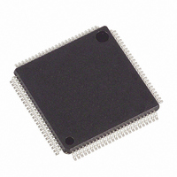
DS21554LB+ Maxim Integrated Products, DS21554LB+ Datasheet - Page 36

DS21554LB+
Manufacturer Part Number
DS21554LB+
Description
IC TXRX E1 5V 100-LQFP
Manufacturer
Maxim Integrated Products
Datasheet
1.DS2154LNA2.pdf
(124 pages)
Specifications of DS21554LB+
Function
Single-Chip Transceiver
Interface
E1, HDLC, J1, T1
Number Of Circuits
1
Voltage - Supply
4.75 V ~ 5.25 V
Current - Supply
75mA
Operating Temperature
0°C ~ 70°C
Mounting Type
Surface Mount
Package / Case
100-LQFP
Includes
Remote and AIS Alarm Detector / Generator
Product
Framer
Number Of Transceivers
1
Data Rate
1.544 Mbps
Supply Voltage (max)
5.25 V
Supply Voltage (min)
4.75 V
Supply Current (max)
75 mA (Typ)
Maximum Operating Temperature
+ 70 C
Minimum Operating Temperature
0 C
Mounting Style
SMD/SMT
Ic Interface Type
Parallel, Serial
Supply Voltage Range
4.75V To 5.25V
Operating Temperature Range
0°C To +70°C
Digital Ic Case Style
LQFP
No. Of Pins
100
Filter Terminals
SMD
Rohs Compliant
Yes
Lead Free Status / RoHS Status
Lead free / RoHS Compliant
Power (watts)
-
Lead Free Status / Rohs Status
Lead free / RoHS Compliant
CCR1: COMMON CONTROL REGISTER 1 (Address = 14 Hex)
5.3.
When CCR1.7 is set to one, the DS21354/DS21554 enter a framer loopback (FLB) mode. See
for more details. This loopback is useful in testing and debugging applications. In FLB, the SCT will loop
data from the transmit side back to the receive side. When FLB is enabled, the following will occur:
1) Data will be transmitted as normal at TPOSO and TNEGO.
2) Data input via RPOSI and RNEGI will be ignored.
3) The RCLK output will be replaced with the TCLK input.
SYMBOL
(MSB)
THDB3
RHDB3
TCRC4
RCRC4
TG802
RG802
FLB
RSM
FLB
Framer Loopback
THDB3
POSITION
CCR1.7
CCR1.6
CCR1.5
CCR1.4
CCR1.3
CCR1.2
CCR1.1
CCR1.0
TG802
Framer Loopback.
0 = loopback disabled
1 = loopback enabled
Transmit HDB3 Enable.
0 = HDB3 disabled
1 = HDB3 enabled
Transmit G.802 Enable. See Section
0 = do not force TCHBLK high during bit 1 of time slot 26
1 = force TCHBLK high during bit 1 of time slot 26
Transmit CRC4 Enable.
0 = CRC4 disabled
1 = CRC4 enabled
Receive Signaling Mode Select.
0 = CAS signaling mode
1 = CCS signaling mode
Receive HDB3 Enable.
0 = HDB3 disabled
1 = HDB3 enabled
Receive G.802 Enable. See Section
0 = do not force RCHBLK high during bit 1 of time slot 26
1=force RCHBLK high during bit 1 of time slot 26
Receive CRC4 Enable.
0 = CRC4 disabled
1 = CRC4 enabled
TCRC4
36 of 124
NAME AND DESCRIPTION
RSM
18
RHDB3
18
for details.
for details.
RG802
RCRC4
Figure 2-1
(LSB)


