DS2151QB+ Maxim Integrated Products, DS2151QB+ Datasheet - Page 6
DS2151QB+
Manufacturer Part Number
DS2151QB+
Description
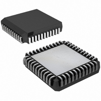
IC TXRX T1 1-CHIP 5V LP 44-PLCC
Manufacturer
Maxim Integrated Products
Datasheet
1.DS2151QB.pdf
(60 pages)
Specifications of DS2151QB+
Function
Single-Chip Transceiver
Interface
T1
Number Of Circuits
1
Voltage - Supply
4.75 V ~ 5.25 V
Current - Supply
65mA
Operating Temperature
0°C ~ 70°C
Mounting Type
Surface Mount
Package / Case
44-LCC, 44-PLCC
Includes
Alarm Detector and Generator, CSU Loop Codes Generator and Detector, DSX-1 and CSU Line Build-Outs Generator
Lead Free Status / RoHS Status
Lead free / RoHS Compliant
Power (watts)
-


2 PIN DESCRIPTION
41–44
1–4,
PIN
10
11
12
13
14
15
16
17
18
19
5
6
7
8
9
RLOS/LOT
AD4–AD7,
AD0–AD3
WR(R/W)
RCHCLK
RCHBLK
ALE(AS)
SYSCLK
RD(DS)
RLCLK
RSYNC
NAME
RLINK
ACLKI
RCLK
DVSS
RSER
CS
C
TYPE
I/O
I/O
—
O
O
O
O
O
O
O
I
I
I
I
I
I
Address/Data Bus. An 8-bit multiplexed address/data bus.
Active-Low Read Input (Data Strobe)
Active-Low Chip Select. Must be low to read or write the port.
Address Latch Enable (Address Strobe). A positive going edge serves to
demultiplex the bus.
Active-Low Write Input (Read/Write)
Receive Link Data. Updated with either FDL data (ESF) or Fs bits (D4) or
Z bits (ZBTSI) one RCLK before the start of a frame. See Section
timing details.
Receive Link Clock. 4kHz or 2kHz (ZBTSI) demand clock for the RLINK
output. See Section
Digital Signal Ground. 0.0V. Should be tied to local ground plane.
Receive Clock. Recovered 1.544MHz clock.
Receive Channel Clock. 192kHz clock that pulses high during the LSB of
each channel. Useful for parallel to serial conversion of channel data,
locating Robbed-Bit signaling bits, and for blocking clocks in DDS
applications. See Section
Receive Serial Data. Received NRZ serial data, updated on rising edges of
RCLK or SYSCLK.
Receive Sync. An extracted pulse, one RCLK wide, is output at this pin,
which identifies either frame (RCR2.4 = 0) or multiframe boundaries
(RCR2.4 = 1). If set to output frame boundaries, then via RCR2.5, RSYNC
can also be set to output double-wide pulses on signaling frames. If the
elastic store is enabled via the CCR1.2, then this pin can be enabled to be
an input via RCR2.3 at which a frame boundary pulse is applied. See
Section
Receive Loss of Sync/Loss of Transmit Clock. A dual function output. If
CCR3.5 = 0, will toggle high when the synchronizer is searching for the T1
frame and multiframe; if CCR3.5 = 1, will toggle high if the TCLK pin has
not toggled for 5µs.
System Clock. 1.544MHz or 2.048MHz clock. Only used when the elastic
store functions are enabled via either CCR1.7 or CCR1.2. Should be tied
low in applications that do not use the elastic store. If tied high for more
than 100µs, will force all output pins (including the parallel port) to tri-
state.
Receive Channel Block. A user-programmable output that can be forced
high or low during any of the 24 T1 channels. Useful for blocking clocks to
a serial UART or LAPD controller in applications where not all T1
channels are used such as Fractional T1, 384kbps service, 768kbps, or
ISDN-PRI. Also useful for locating individual channels in drop-and-insert
applications. See Section
Alternate Clock Input. Upon a receive carrier loss, the clock applied at
this pin (normally 1.544MHz) will be routed to the RCLK pin. If no clock
is routed to this pin, then it should be tied to DVSS via a 1kΩ resistor.
14
for timing details.
6 of 60
14
for timing details.
14
14
for timing details.
for timing details.
FUNCTION
14
for
Related parts for DS2151QB+
Image
Part Number
Description
Manufacturer
Datasheet
Request
R

Part Number:
Description:
MAX7528KCWPMaxim Integrated Products [CMOS Dual 8-Bit Buffered Multiplying DACs]
Manufacturer:
Maxim Integrated Products
Datasheet:
Part Number:
Description:
Single +5V, fully integrated, 1.25Gbps laser diode driver.
Manufacturer:
Maxim Integrated Products
Datasheet:
Part Number:
Description:
Single +5V, fully integrated, 155Mbps laser diode driver.
Manufacturer:
Maxim Integrated Products
Datasheet:
Part Number:
Description:
VRD11/VRD10, K8 Rev F 2/3/4-Phase PWM Controllers with Integrated Dual MOSFET Drivers
Manufacturer:
Maxim Integrated Products
Datasheet:
Part Number:
Description:
Highly Integrated Level 2 SMBus Battery Chargers
Manufacturer:
Maxim Integrated Products
Datasheet:
Part Number:
Description:
Current Monitor and Accumulator with Integrated Sense Resistor; ; Temperature Range: -40°C to +85°C
Manufacturer:
Maxim Integrated Products
Part Number:
Description:
TSSOP 14/A�/RS-485 Transceivers with Integrated 100O/120O Termination Resis
Manufacturer:
Maxim Integrated Products
Part Number:
Description:
TSSOP 14/A�/RS-485 Transceivers with Integrated 100O/120O Termination Resis
Manufacturer:
Maxim Integrated Products
Part Number:
Description:
QFN 16/A�/AC-DC and DC-DC Peak-Current-Mode Converters with Integrated Step
Manufacturer:
Maxim Integrated Products
Part Number:
Description:
TDFN/A/65V, 1A, 600KHZ, SYNCHRONOUS STEP-DOWN REGULATOR WITH INTEGRATED SWI
Manufacturer:
Maxim Integrated Products
Part Number:
Description:
Integrated Temperature Controller f
Manufacturer:
Maxim Integrated Products
Part Number:
Description:
SOT23-6/I�/45MHz to 650MHz, Integrated IF VCOs with Differential Output
Manufacturer:
Maxim Integrated Products
Part Number:
Description:
SOT23-6/I�/45MHz to 650MHz, Integrated IF VCOs with Differential Output
Manufacturer:
Maxim Integrated Products
Part Number:
Description:
EVALUATION KIT/2.4GHZ TO 2.5GHZ 802.11G/B RF TRANSCEIVER WITH INTEGRATED PA
Manufacturer:
Maxim Integrated Products
Part Number:
Description:
QFN/E/DUAL PCIE/SATA HIGH SPEED SWITCH WITH INTEGRATED BIAS RESISTOR
Manufacturer:
Maxim Integrated Products
Datasheet: