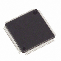
DS21352L Maxim Integrated Products, DS21352L Datasheet - Page 65

DS21352L
Manufacturer Part Number
DS21352L
Description
IC TXRX T1 1-CHIP 3.3V 100-LQFP
Manufacturer
Maxim Integrated Products
Datasheet
1.DS21352L.pdf
(137 pages)
Specifications of DS21352L
Function
Single-Chip Transceiver
Interface
HDLC, T1
Number Of Circuits
1
Voltage - Supply
3.14 V ~ 3.47 V
Current - Supply
75mA
Operating Temperature
0°C ~ 70°C
Mounting Type
Surface Mount
Package / Case
100-LQFP
Includes
DSX-1 and CSU Line Build-Out Generator, HDLC Controller, In-Band Loop Code Generator and Detector
Lead Free Status / RoHS Status
Contains lead / RoHS non-compliant
Power (watts)
-
Available stocks
Company
Part Number
Manufacturer
Quantity
Price
Company:
Part Number:
DS21352L
Manufacturer:
JRC
Quantity:
5 510
Part Number:
DS21352L
Manufacturer:
DALLAS
Quantity:
20 000
Company:
Part Number:
DS21352LN+
Manufacturer:
Maxim Integrated Products
Quantity:
135
14.2 TRANSMIT SIDE
The operation of the transmit elastic store is very similar to the receive side. The transmit side elastic
store is enabled via CCR1.7. A 1.544 MHz (CCR1.4=0) or 2.048 MHz (CCR1.4=1) clock can be applied
to the TSYSCLK input. If the user selects to apply a 2.048 MHz clock to the TSYSCLK pin, then the data
input at TSER will be ignored every fourth channel. Hence channels 1, 5, 9, 13, 17, 21, 25, and 29
(timeslots 0, 4, 8, 12, 16, 20, 24, and 28) will be ignored. The user must supply an 8 kHz frame sync
pulse to the TSSYNC input. Also, in 2.048 MHz applications, the TCHBLK output will be forced high
during the channels ignored by the framer. See Section 21 for more details. Controlled slips in the
transmit elastic store are reported in the RIR2.3 bit and the direction of the slip is reported in the RIR2.5
and RIR2.4 bits.
14.3 ELASTIC STORES INITIALIZATION
There are two elastic store initializations that may be used to improve performance in certain
applications, Elastic Store Reset and Elastic Store Align. Both of these involve the manipulation of the
elastic store’s read and write pointers and are useful primarily in synchronous applications (RSYSCLK /
TSYSCLK are locked to RCLK / TCLK respectively). See table below for details.
Table 14-1 ELASTIC STORE DELAY AFTER INITIALIZATION
Initialization
Receive Elastic Store Reset
Transmit Elastic Store Reset
Receive Elastic Store Align
Transmit Elastic Store Align
14.4 MINIMUM DELAY MODE
Elastic store minimum delay mode may be used when the elastic store’s system clock is locked to its
network clock (i.e., RCLK locked to RSYSCLK for the receive side and TCLK locked to TSYSCLK for
the transmit side). CCR3.7 and CCR3.0 enable the transmit and receive elastic store minimum delay
modes. When enabled the elastic stores will be forced to a maximum depth of 32 bits instead of the
normal 386 bits. This feature is useful primarily in applications that interface to a 2.048MHz bus.
Certain restrictions apply when minimum delay mode is used. In addition to the restriction mentioned
above, RSYNC must be configured as an output when the receive elastic store is in minimum delay mode
and TSYNC must be configured as an output when transmit minimum delay mode is enabled. In a
typical application RSYSCLK and TSYSCLK are locked to RCLK, and RSYNC (frame output mode) is
connected to TSSYNC (frame input mode). All of the slip contention logic in the framer is disabled
(since slips cannot occur). On power–up after the RSYSCLK and TSYSCLK signals have locked to their
respective network clock signals, the elastic store reset bits (CCR7.4 and CCR7.5) should be toggled
from a zero to a one to insure proper operation.
Table 14-2 MINIMUM DELAY MODE CONFIGURATION
Transmit
Receive
15. HDLC CONTROLLER
This device has an enhanced HDLC controller configurable for use with the Facilities Data Link or DS0s.
There are 64 byte buffers in the transmit and receive paths. The user can select any DS0 or multiple
DS0s as well as any specific bits within the DS0(s) to pass through the HDLC controller. Note that
Hardware Requirements
TSYSCLK can be 1.544MHz or 2.048MHz and must
be locked to TCLK (1.544MHz). TSYNC is an output
RSYSCLK can be 1.544MHz or 2.048MHz and must
be locked to RCLK (1.544MHz). RSYNC is an output.
Register. Bit
CCR7.5
CCR7.4
CCR6.6
CCR6.5
65 of 137
Delay
8 Clocks < Delay < 1 Frame
1 Frame < Delay < 2 Frames
½ Frame < Delay < 1 ½ Frames
½ Frame < Delay < 1 ½ Frames
Register Settings
CCR3.0 = 1, CCR1.7 = 1
TCR2.2 = 1
CCR3.7 = 1, CCR1.2 = 1
RCR2.3 = 0


