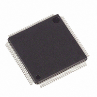
DS21352L Maxim Integrated Products, DS21352L Datasheet - Page 84

DS21352L
Manufacturer Part Number
DS21352L
Description
IC TXRX T1 1-CHIP 3.3V 100-LQFP
Manufacturer
Maxim Integrated Products
Datasheet
1.DS21352L.pdf
(137 pages)
Specifications of DS21352L
Function
Single-Chip Transceiver
Interface
HDLC, T1
Number Of Circuits
1
Voltage - Supply
3.14 V ~ 3.47 V
Current - Supply
75mA
Operating Temperature
0°C ~ 70°C
Mounting Type
Surface Mount
Package / Case
100-LQFP
Includes
DSX-1 and CSU Line Build-Out Generator, HDLC Controller, In-Band Loop Code Generator and Detector
Lead Free Status / RoHS Status
Contains lead / RoHS non-compliant
Power (watts)
-
Available stocks
Company
Part Number
Manufacturer
Quantity
Price
Company:
Part Number:
DS21352L
Manufacturer:
JRC
Quantity:
5 510
Part Number:
DS21352L
Manufacturer:
DALLAS
Quantity:
20 000
Company:
Part Number:
DS21352LN+
Manufacturer:
Maxim Integrated Products
Quantity:
135
16.2 TRANSMIT WAVE SHAPING AND LINE DRIVING
The DS21352/552 uses a set of laser–trimmed delay lines along with a precision Digital–to–Analog
Converter (DAC) to create the waveforms that are transmitted onto the T1 line. The waveforms created
by the DS21352/552 meet the latest ANSI, AT&T, and ITU specifications. See Figure 16-3. The user
will select which waveform is to be generated by properly programming the L2/L1/L0 bits in the Line
Interface Control Register (LICR). The DS21352/552 can set up in a number of various configurations
depending on the application. See Table 16-1.
Table 16-1 LINE BUILD OUT SELECT IN LICR
Due to the nature of the design of the transmitter in the DS21352/552, very little jitter (less then 0.005
UIpp broad-band from 10 Hz to 100 kHz) is added to the jitter present on TCLKI. Also, the waveforms
that they create are independent of the duty cycle of TCLK. The transmitter in the DS21352/552 couples
to the T1 transmit twisted pair via a 1:1.15 or 1:1.36 step up transformer for the DS21552 or a 1:2 step up
transformer for the DS21352 as shown in Figure 16-1. In order for the devices to create the proper
waveforms, this transformer used must meet the specifications listed in Table 16-3.
16.3 JITTER ATTENUATOR
The DS21352/552 contains an onboard jitter attenuator that can be set to a depth of either 32 or 128 bits
via the JABDS bit in the Line Interface Control Register (LICR). The 128 bit mode is used in applications
where large excursions of wander are expected. The 32 bit mode is used in delay sensitive applications.
The characteristics of the attenuation are shown in Figure 16-4. The jitter attenuator can be placed in
either the receive or transmit path via the JAS bit in the LICR. Also, the jitter attenuator can be disabled
(in effect, removed) by setting the DJA bit in the LICR. In order for the jitter attenuator to operate
properly, a 1.544 MHz clock (+50 ppm) must be applied at the MCLK pin or a crystal with similar
characteristics must be applied across the MCLK and XTALD pins. If a crystal is applied across the
MCLK and XTALD pins, then the maximum effective series resistance (ESR) should be 40 Ohms and
capacitors should be placed from each leg of the crystal to the local ground plane as shown in Figure 16–
1. Onboard circuitry adjusts either the recovered clock from the clock/data recovery block or the clock
applied at the TCLKI pin to create a smooth jitter free clock which is used to clock data out of the jitter
attenuator FIFO. It is acceptable to provide a gapped/ bursty clock at the TCLKI pin if the jitter attenuator
is placed on the transmit side. If the incoming jitter exceeds either 120 UIpp (buffer depth is 128 bits) or
28 UIpp (buffer depth is 32 bits), then the DS21352/552 will divide the internal nominal 24.704 MHz
clock by either 15 or 17 instead of the normal 16 to keep the buffer from overflowing. When the device
divides by either 15 or 17, it also sets the Jitter Attenuator Limit Trip (JALT) bit in the Receive
Information Register (RIR3.5).
L2
0
0
0
0
1
1
1
1
L1
0
0
1
1
0
0
1
1
L0
0
1
0
1
0
1
0
1
LINE BUILD OUT
133 feet to266
266 feet to399
399 feet to533
533 feet to655
0 to133 feet/
–22.5 dB
–7.5 dB
–15 dB
84 of 137
DSX–1/0dB CSU
APPLICATION
DSX–1
DSX–1
DSX–1
DSX–1
CSU
CSU
CSU
DS21352/DS21552


