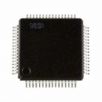
SC16C554BIBM,151 NXP Semiconductors, SC16C554BIBM,151 Datasheet - Page 14

SC16C554BIBM,151
Manufacturer Part Number
SC16C554BIBM,151
Description
IC UART QUAD W/FIFO 64-LQFP
Manufacturer
NXP Semiconductors
Datasheet
1.SC16C554BIBS551.pdf
(58 pages)
Specifications of SC16C554BIBM,151
Number Of Channels
4, QUART
Fifo's
16 Byte
Voltage - Supply
2.5V, 3.3V, 5V
With Auto Flow Control
Yes
With False Start Bit Detection
Yes
With Modem Control
Yes
With Cmos
Yes
Mounting Type
Surface Mount
Package / Case
64-LQFP
Lead Free Status / RoHS Status
Lead free / RoHS Compliant
Other names
568-3267
935279067151
SC16C554BIBM-S
935279067151
SC16C554BIBM-S
Available stocks
Company
Part Number
Manufacturer
Quantity
Price
Company:
Part Number:
SC16C554BIBM,151
Manufacturer:
NXP Semiconductors
Quantity:
10 000
NXP Semiconductors
Table 2.
[1]
SC16C554B_554DB
Product data sheet
Symbol
TXA
TXB
TXC
TXD
TXRDY
V
XTAL1
XTAL2
CC
HVQFN48 package die supply ground is connected to both GND pins and exposed center pad. GND pins must be connected to supply
ground for proper device operation. For enhanced thermal, electrical, and board level performance, the exposed pad needs to be
soldered to the board using a corresponding thermal pad on the board and for proper heat conduction through the board, thermal vias
need to be incorporated in the PCB in the thermal pad region.
Pin description
Pin
PLCC68 LQFP64 LQFP80 HVQFN48
17
19
51
53
39
13, 30,
47, 64
35
36
8
10
39
41
-
4, 21,
35, 52
25
26
…continued
29
32
69
72
55
5, 25,
45, 65
50
51
All information provided in this document is subject to legal disclaimers.
5 V, 3.3 V and 2.5 V quad UART, 5 Mbit/s (max.) with 16-byte FIFOs
6
8
32
34
-
2, 28
18
19
Rev. 4 — 8 June 2010
Type
O
O
O
O
O
I
I
O
Description
Transmit data A, B, C, D. These outputs are
associated with individual serial transmit channel data
from the SC16C554B/554DB. The TX signal will be a
logic 1 during reset, idle (no data), or when the
transmitter is disabled. During the local Loopback
mode, the TXn output pin is disabled and TX data is
internally connected to the UART RX input.
Transmit Ready (active LOW). TXRDY contains the
wire-ORed status of all four transmit channel FIFOs,
TXRDYA to TXRDYD. A logic 0 indicates a buffer ready
status, that is, at least one location is empty and
available in one of the TX channels (A to D). This pin
goes to a logic 1 when all four channels have no more
empty locations in the TX FIFO or THR. Individual
channel TX status can be read by examining individual
internal registers via CS and A0 to A4 pin functions.
The TXRDY pin is not available on the HVQFN48
package.
Power supply inputs.
Crystal or external clock input. Functions as a crystal
input or as an external clock input. A crystal can be
connected between this pin and XTAL2 to form an
internal oscillator circuit (see
an external clock can be connected to this pin to
provide custom data rates. (See
“Programmable baud rate
Output of the crystal oscillator or buffered clock.
(See also XTAL1.) Crystal oscillator output or buffered
clock output.
SC16C554B/554DB
generator”.)
Figure
Section 6.6
© NXP B.V. 2010. All rights reserved.
13). Alternatively,
14 of 58


