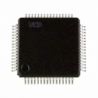
SC16C554BIBM,151 NXP Semiconductors, SC16C554BIBM,151 Datasheet - Page 29

SC16C554BIBM,151
Manufacturer Part Number
SC16C554BIBM,151
Description
IC UART QUAD W/FIFO 64-LQFP
Manufacturer
NXP Semiconductors
Datasheet
1.SC16C554BIBS551.pdf
(58 pages)
Specifications of SC16C554BIBM,151
Number Of Channels
4, QUART
Fifo's
16 Byte
Voltage - Supply
2.5V, 3.3V, 5V
With Auto Flow Control
Yes
With False Start Bit Detection
Yes
With Modem Control
Yes
With Cmos
Yes
Mounting Type
Surface Mount
Package / Case
64-LQFP
Lead Free Status / RoHS Status
Lead free / RoHS Compliant
Other names
568-3267
935279067151
SC16C554BIBM-S
935279067151
SC16C554BIBM-S
Available stocks
Company
Part Number
Manufacturer
Quantity
Price
Company:
Part Number:
SC16C554BIBM,151
Manufacturer:
NXP Semiconductors
Quantity:
10 000
NXP Semiconductors
SC16C554B_554DB
Product data sheet
7.3.1.1 Mode 0 (FCR bit 3 = 0)
7.3.1.2 Mode 1 (FCR bit 3 = 1)
7.2.1 IER versus Receive FIFO interrupt mode operation
7.2.2 IER versus Receive/Transmit FIFO polled mode operation
7.3.1 DMA mode
7.3 FIFO Control Register (FCR)
When the receive FIFO (FCR[0] = logic 1), and receive interrupts (IER[0] = logic 1) are
enabled, the receive interrupts and register status will reflect the following:
When FCR[0] = logic 1, resetting IER[3:0] enables the SC16C554B/554DB in the FIFO
polled mode of operation. Since the receiver and transmitter have separate bits in the
LSR, either or both can be used in the polled mode by selecting respective transmit or
receive control bit(s).
This register is used to enable the FIFOs, clear the FIFOs, set the receive FIFO trigger
levels, and select the DMA mode.
Set and enable the interrupt for each single transmit or receive operation, and is similar to
the 16C454 mode. Transmit Ready (TXRDY) will go to a logic 0 whenever an empty
transmit space is available in the Transmit Holding Register (THR). Receive Ready
(RXRDY) will go to a logic 0 whenever the Receive Holding Register (RHR) is loaded with
a character.
Set and enable the interrupt in a block mode operation. The transmit interrupt is set when
there are one or more FIFO locations empty. The receive interrupt is set when the receive
FIFO fills to the programmed trigger level. However, the FIFO continues to fill regardless
of the programmed level until the FIFO is full. RXRDY remains a logic 0 as long as the
FIFO fill level is above the programmed trigger level.
•
•
•
•
•
•
•
•
The receive data available interrupts are issued to the external CPU when the FIFO
has reached the programmed trigger level. It will be cleared when the FIFO drops
below the programmed trigger level.
FIFO status will also be reflected in the user accessible ISR register when the FIFO
trigger level is reached. Both the ISR register status bit and the interrupt will be
cleared when the FIFO drops below the trigger level.
The data ready bit (LSR[0]) is set as soon as a character is transferred from the shift
register to the receive FIFO. It is reset when the FIFO is empty.
LSR[0] will be a logic 1 as long as there is one byte in the receive FIFO.
LSR[4:1] will provide the type of errors encountered, if any.
LSR[5] will indicate when the transmit FIFO is empty.
LSR[6] will indicate when both the transmit FIFO and Transmit Shift Register are
empty.
LSR[7] will indicate any FIFO data errors.
All information provided in this document is subject to legal disclaimers.
5 V, 3.3 V and 2.5 V quad UART, 5 Mbit/s (max.) with 16-byte FIFOs
Rev. 4 — 8 June 2010
SC16C554B/554DB
© NXP B.V. 2010. All rights reserved.
29 of 58


