PC16552DV/NOPB National Semiconductor, PC16552DV/NOPB Datasheet - Page 15
PC16552DV/NOPB
Manufacturer Part Number
PC16552DV/NOPB
Description
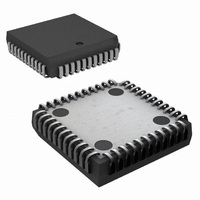
IC UART DUAL WITH FIFO 44-PLCC
Manufacturer
National Semiconductor
Datasheet
1.PC16552DVNOPB.pdf
(22 pages)
Specifications of PC16552DV/NOPB
Features
False-start Bit Detection
Number Of Channels
2, DUART
Fifo's
16 Byte
Voltage - Supply
5V
With False Start Bit Detection
Yes
With Modem Control
Yes
Mounting Type
Surface Mount
Package / Case
44-LCC (J-Lead)
No. Of Channels
2
Data Rate
1.5Mbps
Uart Features
Independently Controlled Transmit, Receive, Line Status, And Data Set Interrupts
Supply Voltage Range
4.5V To 5.5V
Rohs Compliant
Yes
Lead Free Status / RoHS Status
Lead free / RoHS Compliant
Other names
*PC16552DV
*PC16552DV/NOPB
PC16552DV
*PC16552DV/NOPB
PC16552DV
Available stocks
Company
Part Number
Manufacturer
Quantity
Price
Company:

Part Number:
PC16552DV/NOPB
Manufacturer:
TI
Quantity:
7 782
Company:
Part Number:
PC16552DV/NOPB
Manufacturer:
NSC
Quantity:
12 464
Company:
Part Number:
PC16552DV/NOPB
Manufacturer:
Texas Instruments
Quantity:
10 000


8 0 Registers
Two identical register sets one for each channel are in the
DUART All register descriptions in this section apply to the
register sets in both channels
8 1 LINE CONTROL REGISTER
The system programmer specifies the format of the asyn-
chronous data communications exchange and sets the Divi-
sor Latch Access bit via the Line Control Register (LCR)
This is a read and write register Table II shows the contents
of the LCR Details on each bit follow
Bits 0 and 1 These two bits specify the number of data bits
in each transmitted or received serial character The encod-
ing of bits 0 and 1 is as follows
Bit 2 This bit specifies the number of Stop bits transmitted
with each serial character If bit 2 is a logic 0 one Stop bit is
generated in the transmitted data If bit 2 is a logic 1 when a
5-bit data length is selected one and a half Stop bits are
generated If bit 2 is a logic 1 when either a 6- 7- or 8-bit
word length is selected two Stop bits are generated The
receiver checks the first Stop bit only regardless of the
number of Stop bits selected
Bit 3 This bit is the Parity Enable bit When bit 3 is a logic 1
a Parity bit is generated (transmit data) or checked (receive
data) between the last data bit and Stop bit of the serial
data (The Parity bit is used to produce an even or odd
number of 1s when the data bits and the Parity bit are
summed )
Bit 4 This bit is the Even Parity Select bit When parity is
enabled and bit 4 is a logic 0 an odd number of logic 1s is
transmitted or checked in the data word bits and Parity bit
When parity is enabled and bit 4 is a logic 1 an even num-
ber of logic 1s is transmitted or checked
Bit 5 This bit is the Stick Parity bit When parity is enabled it
is used in conjunction with bit 4 to select Mark or Space
Parity When bits 3 4 and 5 are logic 1 the Parity bit is
transmitted and checked as a logic 0 (Space Parity) If bits 3
and 5 are 1 and bit 4 is a logic 0 then the Parity bit is
transmitted and checked as a logic 1 (Mark Parity) If bit 5 is
a logic 0 Stick Parity is disabled
Bit 6 This bit is the Break Control bit It causes a break
condition to be transmitted to the receiving UART When it
is set to a logic 1 the serial output (SOUT) is forced to the
Spacing state (logic 0) The break is disabled by setting bit 6
to a logic 0 The Break Control bit acts only on SOUT and
has no effect on the transmitter logic
Bit 1
0
0
1
1
Composite Serial Data
(Continued)
Bit 0
0
1
0
1
Data Length
5 Bits
6 Bits
7 Bits
8 Bits
TL C 9426– 21
15
Note This feature enables the CPU to alert a terminal in a computer com-
1 Load an all 0s pad character in response to THRE
2 Set break after the next THRE
3 Wait for the transmitter to be idle (TEMT
During the break the Transmitter can be used as a character timer to accu-
rately establish the break duration
Bit 7 This bit is the Divisor Latch Access Bit (DLAB) It must
be set high (logic 1) to access the Divisor Latches of the
Baud Generator or the Alternate Function Register during a
Read or Write operation It must be set low (logic 0) to ac-
cess any other register
8 2 TYPICAL CLOCK CIRCUITS
Note These R and C values are approximate and may vary 2 x depending
normal transmission has to be restored
3 1 MHz
1 8 MHz
Crystal
munications system If the following sequence is followed no errone-
ous or extraneous characters will be transmitted because of the
break
on the crystal characteristics All crystal circuits should be designed
specifically for the system
Typical Crystal Oscillator Network (Note)
1 M
1 M
R
P
R
1 5k
1 5k
X2
10 – 30 pF
10 – 30 pF
e
C
1
1) and clear break when
40– 60 pF
40– 60 pF
TL C 9426 – 18
TL C 9426 – 19
C
2
Related parts for PC16552DV/NOPB
Image
Part Number
Description
Manufacturer
Datasheet
Request
R

Part Number:
Description:
UART IC
Manufacturer:
National Semiconductor
Datasheet:

Part Number:
Description:
National Semiconductor [8-Bit D/A Converter]
Manufacturer:
National Semiconductor
Datasheet:
Part Number:
Description:
National Semiconductor [Media Coprocessor]
Manufacturer:
National Semiconductor
Datasheet:
Part Number:
Description:
Digitally Controlled Tone and Volume Circuit with Stereo Audio Power Amplifier, Microphone Preamp Stage and National 3D Sound
Manufacturer:
National Semiconductor
Datasheet:
Part Number:
Description:
Digitally Controlled Tone and Volume Circuit with Stereo Audio Power Amplifier, Microphone Preamp Stage and National 3D Sound
Manufacturer:
National Semiconductor
Datasheet:
Part Number:
Description:
AC97 Rev 2 Codec with Sample Rate Conversion and National 3D Sound
Manufacturer:
National Semiconductor
Part Number:
Description:
Manufacturer:
National Semiconductor
Datasheet:
Part Number:
Description:
Manufacturer:
National Semiconductor
Datasheet:
Part Number:
Description:
General Purpose, Low Voltage, Low Power, Rail-to-Rail Output Operational Amplifiers
Manufacturer:
National Semiconductor
Datasheet:
Part Number:
Description:
8-bit 20 MSPS flash A/D converter.
Manufacturer:
National Semiconductor
Datasheet:
Part Number:
Description:
Low Noise Quad Operational Amplifier
Manufacturer:
National Semiconductor
Datasheet:
Part Number:
Description:
Quad Differential Line Receivers
Manufacturer:
National Semiconductor
Datasheet:
Part Number:
Description:
Quad High Speed Trapezoidal? Bus Transceiver
Manufacturer:
National Semiconductor
Datasheet:
Part Number:
Description:
Dual Line Receiver
Manufacturer:
National Semiconductor
Datasheet: