PC16552DV/NOPB National Semiconductor, PC16552DV/NOPB Datasheet - Page 17
PC16552DV/NOPB
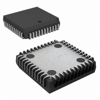
Manufacturer Part Number
PC16552DV/NOPB
Description
IC UART DUAL WITH FIFO 44-PLCC
Manufacturer
National Semiconductor
Datasheet
1.PC16552DVNOPB.pdf
(22 pages)
Specifications of PC16552DV/NOPB
Features
False-start Bit Detection
Number Of Channels
2, DUART
Fifo's
16 Byte
Voltage - Supply
5V
With False Start Bit Detection
Yes
With Modem Control
Yes
Mounting Type
Surface Mount
Package / Case
44-LCC (J-Lead)
No. Of Channels
2
Data Rate
1.5Mbps
Uart Features
Independently Controlled Transmit, Receive, Line Status, And Data Set Interrupts
Supply Voltage Range
4.5V To 5.5V
Rohs Compliant
Yes
Lead Free Status / RoHS Status
Lead free / RoHS Compliant
Other names
*PC16552DV
*PC16552DV/NOPB
PC16552DV
*PC16552DV/NOPB
PC16552DV
Available stocks
Company
Part Number
Manufacturer
Quantity
Price
Company:

Part Number:
PC16552DV/NOPB
Manufacturer:
TI
Quantity:
7 782
Company:
Part Number:
PC16552DV/NOPB
Manufacturer:
NSC
Quantity:
12 464
Company:
Part Number:
PC16552DV/NOPB
Manufacturer:
Texas Instruments
Quantity:
10 000


Baud Rate
8 0 Registers
Bit 4 This bit is the Break Interrupt (BI) indicator Bit 4 is set
to a logic 1 whenever the received data input is held in the
Spacing (logic 0) state for longer than a full word transmis-
sion time (that is the total time of Start bit
Parity
CPU reads the contents of the Line Status Register or when
the next valid character is loaded into the Receiver Buffer
Register In the FIFO Mode this condition is associated with
the particular character in the FIFO it applies to It is re-
vealed to the CPU when its associated character is at the
top of the FIFO When break occurs only one zero character
is loaded into the FIFO The next character transfer is en-
abled after SIN goes to the marking state and receives the
next valid start bit
Note Bits 1 through 4 are the error conditions that produce a Receiver Line
Bit 5 This bit is the Transmitter Holding Register Empty
(THRE) indicator In the 16450 mode bit 5 indicates that the
associated serial channel is ready to accept a new charac-
ter for transmission In addition this bit causes the DUART
to issue an interrupt to the CPU when the Transmit Holding
Register Empty Interrupt enable is set high The THRE bit is
set to a logic 1 when a character is transferred from the
Transmitter Holding Register into the Transmitter Shift Reg-
ister The bit is reset to logic 0 concurrently with the loading
of the Transmitter Holding Register by the CPU In the FIFO
mode this bit is set when the XMIT FIFO is empty it is
cleared when at least 1 byte is written to the XMIT FIFO
Bit 6 This bit is the Transmitter Empty (TEMT) indicator Bit
6 is set to a logic 1 whenever the Transmitter Holding Regis-
ter (THR) and the Transmitter Shift Register (TSR) are both
empty It is reset to a logic 0 whenever either the THR or
TSR contains a data character In the FIFO mode this bit is
set to one whenever the transmitter FIFO and shift register
are both empty
Note For baud rates of 250k 300k 375k 500k 750k and 1 5M using a 24 MHz crystal causes minimal error
128000
19200
38400
56000
134 5
1200
1800
2000
2400
3600
4800
7200
9600
110
150
300
600
50
75
Status interrupt whenever any of the corresponding conditions are
detected and the interrupt is enabled
a
Stop bits) The BI indicator is reset whenever the
Decimal Divisor
for 16
2304
1536
1047
857
768
384
192
96
64
58
48
32
24
16
12
1 8432 MHz Crystal
c
6
3
2
(Continued)
Clock
Percent Error
0 026
0 058
TABLE IV Baud Rates Divisors and Crystals
0 69
2 86
a
data bits
Decimal Divisor
for 16
a
3840
2560
1745
1428
1280
640
320
160
107
96
80
53
40
27
20
10
c
5
3 072 MHz Crystal
17
Clock
Bit 7 In the 16450 Mode this is a 0 In the FIFO Mode LSR7
is set when there is at least one parity error framing error or
break indication in the FIFO LSR7 is cleared when the CPU
reads the LSR if there are no subsequent errors in the
FIFO
Note The Line Status Register is intended for read operations only Writing
8 5 FIFO CONTROL REGISTER
This is a write only register at the same location as the IIR
(the IIR is a read only register) This register is used to en-
able the FIFOs clear the FIFOs set the RCVR FIFO trigger
level and select the type of DMA signalling
Bit 0 Writing a 1 to FCR0 enables both the XMIT and RCVR
FIFOs Resetting FCR0 will clear all bytes in both FIFOs
When changing from FIFO Mode to 16450 Mode and vice
versa data is automatically cleared from the FIFOs This bit
must be a 1 when other FCR bits are written to or they will
not be programmed
Bit 1 Writing a 1 to FCR1 clears all bytes in the RCVR FIFO
and resets its counter logic to 0 The shift register is not
cleared The 1 that is written to this bit position is self-clear-
ing
Bit 2 Writing a 1 to FCR2 clears all bytes in the XMIT FIFO
and resets its counter logic to 0 The shift register is not
cleared The 1 that is written to this bit position is self-clear-
ing
Bit 3 Writing a 1 to FCR3 causes RXRDY and TXRDY oper-
ations to change from mode 0 to mode 1 if FCR0
RXRDY Mode 0 When in the 16450 Mode (FCR0
in the FIFO Mode (FCR0
least 1 character in the RCVR FIFO or RCVR Buffer Regis-
ter the RXRDY pin will go low active Once active the
RXRDY pin will go inactive when there are no more charac-
ters in the FIFO or Buffer Register
to this register is not recommended as this operation is only used for
factory testing In the FIFO mode the user must load a data byte into
the Rx FIFO in order to write to LSR2–4 LSR0 and LSR7 cannot be
written to in the FIFO mode
Percent Error
0 026
0 034
0 312
0 628
1 23
Decimal Divisor
for 16
e
1 FCR3
23040
15360
10473
8565
7680
3840
1920
920
640
576
480
320
240
160
120
60
30
21
18 432 MHz Crystal
c
9
Clock
e
0) and there is at
Percent Error
e
2 04
e
1
0) or
Related parts for PC16552DV/NOPB
Image
Part Number
Description
Manufacturer
Datasheet
Request
R

Part Number:
Description:
UART IC
Manufacturer:
National Semiconductor
Datasheet:

Part Number:
Description:
National Semiconductor [8-Bit D/A Converter]
Manufacturer:
National Semiconductor
Datasheet:
Part Number:
Description:
National Semiconductor [Media Coprocessor]
Manufacturer:
National Semiconductor
Datasheet:
Part Number:
Description:
Digitally Controlled Tone and Volume Circuit with Stereo Audio Power Amplifier, Microphone Preamp Stage and National 3D Sound
Manufacturer:
National Semiconductor
Datasheet:
Part Number:
Description:
Digitally Controlled Tone and Volume Circuit with Stereo Audio Power Amplifier, Microphone Preamp Stage and National 3D Sound
Manufacturer:
National Semiconductor
Datasheet:
Part Number:
Description:
AC97 Rev 2 Codec with Sample Rate Conversion and National 3D Sound
Manufacturer:
National Semiconductor
Part Number:
Description:
Manufacturer:
National Semiconductor
Datasheet:
Part Number:
Description:
Manufacturer:
National Semiconductor
Datasheet:
Part Number:
Description:
General Purpose, Low Voltage, Low Power, Rail-to-Rail Output Operational Amplifiers
Manufacturer:
National Semiconductor
Datasheet:
Part Number:
Description:
8-bit 20 MSPS flash A/D converter.
Manufacturer:
National Semiconductor
Datasheet:
Part Number:
Description:
Low Noise Quad Operational Amplifier
Manufacturer:
National Semiconductor
Datasheet:
Part Number:
Description:
Quad Differential Line Receivers
Manufacturer:
National Semiconductor
Datasheet:
Part Number:
Description:
Quad High Speed Trapezoidal? Bus Transceiver
Manufacturer:
National Semiconductor
Datasheet:
Part Number:
Description:
Dual Line Receiver
Manufacturer:
National Semiconductor
Datasheet: