PC16552DV/NOPB National Semiconductor, PC16552DV/NOPB Datasheet - Page 18
PC16552DV/NOPB
Manufacturer Part Number
PC16552DV/NOPB
Description
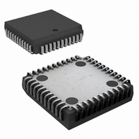
IC UART DUAL WITH FIFO 44-PLCC
Manufacturer
National Semiconductor
Datasheet
1.PC16552DVNOPB.pdf
(22 pages)
Specifications of PC16552DV/NOPB
Features
False-start Bit Detection
Number Of Channels
2, DUART
Fifo's
16 Byte
Voltage - Supply
5V
With False Start Bit Detection
Yes
With Modem Control
Yes
Mounting Type
Surface Mount
Package / Case
44-LCC (J-Lead)
No. Of Channels
2
Data Rate
1.5Mbps
Uart Features
Independently Controlled Transmit, Receive, Line Status, And Data Set Interrupts
Supply Voltage Range
4.5V To 5.5V
Rohs Compliant
Yes
Lead Free Status / RoHS Status
Lead free / RoHS Compliant
Other names
*PC16552DV
*PC16552DV/NOPB
PC16552DV
*PC16552DV/NOPB
PC16552DV
Available stocks
Company
Part Number
Manufacturer
Quantity
Price
Company:

Part Number:
PC16552DV/NOPB
Manufacturer:
TI
Quantity:
7 782
Company:
Part Number:
PC16552DV/NOPB
Manufacturer:
NSC
Quantity:
12 464
Company:
Part Number:
PC16552DV/NOPB
Manufacturer:
Texas Instruments
Quantity:
10 000


Mode
FIFO
Bit 3 Bit 2 Bit 1 Bit 0
Only
8 0 Registers
RXRDY Mode 1 In the FIFO Mode (FCR0
FCR3
reached the RXRDY pin will go low active Once it is acti-
vated it will go inactive when there are no more characters
in the FIFO
TXRDY Mode 0 In the 16450 Mode (FCR0
FIFO Mode (FCR0
characters in the XMIT FIFO or XMIT Holding Register the
TXRDY pin will go low active Once active the TXRDY pin
will go inactive after the first character is loaded into the
XMIT FIFO or Holding Register
TXRDY Mode 1 In the FIFO Mode (FCR0
and when there are no characters in the XMIT FIFO the
TXRDY pin will go low active This pin will become inactive
when the XMIT FIFO is completely full
Bit 4 5 FCR4 to FCR5 are reserved for future use
Bit 6 7 FCR6 and FCR7 are used to designate the interrupt
trigger level When the number of bytes in the RCVR FIFO
equals the designated interrupt trigger level a Received
Data Available Interrupt is activated This interrupt must be
enabled by setting IER0
0
0
0
1
0
0
e
FCR Bits
Identification
0
1
1
1
0
0
7 6
0 0
0 1
1 0
1 1
Interrupt
Register
1 and the trigger level or the timeout has been
0
1
0
0
1
0
1
0
0
0
0
0
e
(Continued)
1 FCR3
Priority
Highest Receiver Line Status
Second Received Data Available Receiver Data Available or Trigger
Second Character Timeout
Fourth
Level
Third
Trigger Level (Bytes)
e
None
Indication
Transmitter Holding
Register Empty
MODEM Status
RCVR FIFO
0) when there are no
Interrupt Type
01
04
08
14
e
TABLE V Interrupt Control Functions
e
e
1 FCR3
1) when the
0) or in the
e
1)
Interrupt Set and Reset Functions
None
Overrun Error or Parity Error or
Framing Error or Break Interrupt
Level Reached
No Characters Have Been
Removed from or Input to the
RCVR FIFO During the Last 4 Char
Times and There is at Least 1 Char
in it During This Time
Transmitter Holding
Register Empty
Clear to Send or Data Set Ready or
Ring Indicator or Data Carrier
Detect
18
8 6 INTERRUPT IDENTIFICATION REGISTER
In order to provide minimum software overhead during data
character transfers each serial channel of the DUART prior-
itizes interrupts into four levels and records these in the
Interrupt Identification Register The four levels of interrupt
conditions in order of priority are Receiver Line Status Re-
ceived Data Ready Transmitter Holding Register Empty
and MODEM Status
When the CPU reads the IIR the associated DUART serial
channel freezes all interrupts and indicates the highest pri-
ority pending interrupt to the CPU While this CPU access is
occurring the associated DUART serial channel records
new interrupts but does not change its current indication
until the access is complete Table II shows the contents of
the IIR Details on each bit follow
Bit 0 This bit can be used in a prioritized interrupt environ-
ment to indicate whether an interrupt is pending When bit 0
is a logic 0 an interrupt is pending and the IIR contents may
be used as a pointer to the appropriate interrupt service
routine When bit 0 is a logic 1 no interrupt is pending
Bits 1 and 2 These two bits of the IIR identify the highest
priority interrupt pending from those shown in Table V
Bit 3 In the 16450 Mode this bit is 0 In the FIFO Mode this
bit is set along with bit 2 when a timeout interrupt is pending
Bits 4 and 5 These two bits of the IIR are always logic 0
Bits 6 and 7 These two bits are set when FCR0
(FIFO Mode enabled )
Interrupt Source
Reading the Line Status
Register
Reading the Receiver Buffer
Register or the FIFO Drops
below the Trigger Level
Reading the Receiver
Buffer Register
Reading the IIR Register (if
Source of Interrupt) or Writing
into the Transmitter Holding
Register
Reading the MODEM
Status Register
Interrupt Reset Control
e
1
Related parts for PC16552DV/NOPB
Image
Part Number
Description
Manufacturer
Datasheet
Request
R

Part Number:
Description:
UART IC
Manufacturer:
National Semiconductor
Datasheet:

Part Number:
Description:
National Semiconductor [8-Bit D/A Converter]
Manufacturer:
National Semiconductor
Datasheet:
Part Number:
Description:
National Semiconductor [Media Coprocessor]
Manufacturer:
National Semiconductor
Datasheet:
Part Number:
Description:
Digitally Controlled Tone and Volume Circuit with Stereo Audio Power Amplifier, Microphone Preamp Stage and National 3D Sound
Manufacturer:
National Semiconductor
Datasheet:
Part Number:
Description:
Digitally Controlled Tone and Volume Circuit with Stereo Audio Power Amplifier, Microphone Preamp Stage and National 3D Sound
Manufacturer:
National Semiconductor
Datasheet:
Part Number:
Description:
AC97 Rev 2 Codec with Sample Rate Conversion and National 3D Sound
Manufacturer:
National Semiconductor
Part Number:
Description:
Manufacturer:
National Semiconductor
Datasheet:
Part Number:
Description:
Manufacturer:
National Semiconductor
Datasheet:
Part Number:
Description:
General Purpose, Low Voltage, Low Power, Rail-to-Rail Output Operational Amplifiers
Manufacturer:
National Semiconductor
Datasheet:
Part Number:
Description:
8-bit 20 MSPS flash A/D converter.
Manufacturer:
National Semiconductor
Datasheet:
Part Number:
Description:
Low Noise Quad Operational Amplifier
Manufacturer:
National Semiconductor
Datasheet:
Part Number:
Description:
Quad Differential Line Receivers
Manufacturer:
National Semiconductor
Datasheet:
Part Number:
Description:
Quad High Speed Trapezoidal? Bus Transceiver
Manufacturer:
National Semiconductor
Datasheet:
Part Number:
Description:
Dual Line Receiver
Manufacturer:
National Semiconductor
Datasheet: