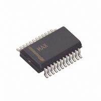
MAX9511CEG+ Maxim Integrated Products, MAX9511CEG+ Datasheet - Page 10

MAX9511CEG+
Manufacturer Part Number
MAX9511CEG+
Description
IC INTERFACE VGA 24-QSOP
Manufacturer
Maxim Integrated Products
Type
RGBHV Driverr
Datasheet
1.MAX9511CEGT.pdf
(15 pages)
Specifications of MAX9511CEG+
Applications
Driver
Number Of Circuits
3
Slew Rate
1100 V/µs
Current - Supply
38mA
Current - Output / Channel
40mA
Voltage - Supply, Single/dual (±)
4.5 V ~ 5.5 V
Mounting Type
Surface Mount
Package / Case
24-QSOP
Operating Supply Voltage
4.5 V to 5.5 V
Maximum Operating Temperature
+ 70 C
Maximum Power Dissipation
762 mW
Minimum Operating Temperature
0 C
Mounting Style
SMD/SMT
Lead Free Status / RoHS Status
Lead free / RoHS Compliant
RGBHV Driver with EMI Suppression
The MAX9511 has separate, noninverting, vertical and
horizontal sync buffers. Both sync inputs can level-shift
an input as low as 2.3V to a 5V output. Both sync drivers
have hysteresis at their input to prevent “chatter” in their
outputs. The sync output drivers have a 55Ω (typ) out-
put impedance (R
used for vertical and horizontal sync in most applica-
tions. Both sync inputs are pulled to DGND through a
47kΩ resistor if the controller’s SYNC source goes high
impedance, or if the inputs are left floating, avoiding
ambiguous output conditions.
EMI can result from rapid transitions of the sync or the
video signals. To reduce the rise and fall times of the
sync signal, additional capacitance may be added to
the sync outputs. Adding additional capacitance may
require “recentering” the display.
The MAX9511 bidirectional display data channel (DDC)
level translator allows for a lower voltage video controller
logic to operate with a higher voltage external monitor
logic. Power supplied at V
voltage thresholds while power supplied at V
the DDC output thresholds. Two Schottky-clamped npn
transistors shift the lower level DDC inputs to higher
logic-level outputs.
DDC_CLK_OUT and DDC_DATA_OUT are pulled to
V
conditions when left floating. At shutdown, DDC inputs
can still respond to external commands.
The MAX9511 outputs are slew-rate limited to reduce
EMI. Slew-rate limiting affects the large-signal bandwidth
(LSBW) more than the small-signal bandwidth (SSBW),
and can be scaled according to the following formula:
where V
and LSBW(-3dB) is the -3dB bandwidth.
The slew rate of the MAX9511 is controlled by a resistor
between RX and AGND. The resistor (R
ied to optimize the EMI suppression to the display reso-
lution while preserving the display quality. The R
range is approximately 7kΩ for maximum slew rate and
50kΩ for minimum slew rate (see Figure 3). Slew-rate
limiting can be approximated by:
10
DD1
______________________________________________________________________________________
by internal pullup resistors to prevent ambiguous
OUT
is the output signal’s peak-to-peak voltage
LSBW
SR
Vertical and Horizontal SYNC
=
SO
(
Display Data Channel (DDC)
1030
−
3
) to match the cable impedance
dB
⎛
⎜
⎝
)
7000
=
R
DD2
RX
2
×
Slew-Rate Limiting
⎞
⎟
⎠
defines the DDC input
π
( /
V
S
×
R
V
µ
OUT
s
)
RX
) can be var-
DD1
defines
RX
The MAX9511 features a low-power shutdown mode for
battery-powered/portable applications. Shutdown
reduces the quiescent current of the video and sync dri-
vers. Connecting SHDN to ground (DGND) disables the
outputs and places the MAX9511 into a low-power shut-
down mode. SHDN has a 330kΩ (typ) internal pulldown
resistor to DGND. Connect SHDN to V
operation.
When the MAX9511 connects to devices of different
resolutions, different slew rates should be used. The
slew rate of the MAX9511 is adjustable by varying R
between 7kΩ and 50kΩ. By selecting a valid R
for a resolution, the MAX9511 minimizes the EMI and
optimizes the video output quality. Shown are two con-
figurations to adjust slew rates using different R
ues for different video resolutions.
Figure 4 shows how to customize slew rates for three res-
olutions. This circuit provides three predetermined slew
rates by paralleling resistors to create three R
The combination is controlled by a digital command from
the video controller through a switch. This requires that
the sample clock rates used by different resolutions are
close. The sync bandwidth-limiting capacitors (C
are set for the highest resolution.
Figure 3. Slew Rate vs. R RX
1600
1400
1200
1000
800
600
400
200
0
0
Applications Information
Customizing Slew Rates for
10
SLEW RATE vs. R
20
R
RX
Different Resolutions
(kΩ)
30
RX
40
DD2
Shutdown
50
for normal
RX
RX
RX
values.
SYNC
value
val-
RX
)


