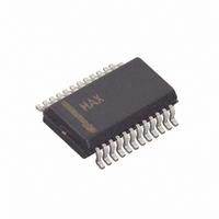
MAX9511CEG+ Maxim Integrated Products, MAX9511CEG+ Datasheet - Page 4

MAX9511CEG+
Manufacturer Part Number
MAX9511CEG+
Description
IC INTERFACE VGA 24-QSOP
Manufacturer
Maxim Integrated Products
Type
RGBHV Driverr
Datasheet
1.MAX9511CEGT.pdf
(15 pages)
Specifications of MAX9511CEG+
Applications
Driver
Number Of Circuits
3
Slew Rate
1100 V/µs
Current - Supply
38mA
Current - Output / Channel
40mA
Voltage - Supply, Single/dual (±)
4.5 V ~ 5.5 V
Mounting Type
Surface Mount
Package / Case
24-QSOP
Operating Supply Voltage
4.5 V to 5.5 V
Maximum Operating Temperature
+ 70 C
Maximum Power Dissipation
762 mW
Minimum Operating Temperature
0 C
Mounting Style
SMD/SMT
Lead Free Status / RoHS Status
Lead free / RoHS Compliant
RGBHV Driver with EMI Suppression
ELECTRICAL CHARACTERISTICS (continued)
(V
values are at T
Note 1: This is the voltage at which the input termination switches; V
Note 2: Measured between the 10% to 90% points on rising or falling edge.
Note 3: Not production tested. Guaranteed by design.
Note 4: Measured from the END of overshoot/undershoot to ±5% of final value.
Note 5: V
Note 6: Linearity error is the maximum difference between the actual and measured output of a video ramp. Done in accordance
Note 7: Linearity error measured as percentage of full scale.
Note 8: Propagation delay is the time difference between the V
(V
4
Rise/Fall Time
Propagation Delay
Enable Time
Disable Time
CC
CC
_______________________________________________________________________________________
-1
-2
-3
-4
-5
-6
-7
3
2
1
0
= 5V, V
= 5V, V
0.1
PARAMETER
with VESA Test Procedure, Version 1, 6/11/2001.
V
T
A
IN
OUT
= T
LARGE-SIGNAL BANDWIDTH
= 700mV with a rise time >1ns.
= 1.6V
DD1
DD1
MIN
A
1
to T
= +25°C.)
P-P
= 5V, V
vs. FREQUENCY
= 5V, V
FREQUENCY (MHz)
MAX
10
DD2
DD2
= 3V, R
= SHDN = 3V, R
100
t
SYMBOL
PLH
t
R
L
, t
/t
= 150Ω to AGND, R
F
1000
PHL
All SYNC outputs
(Notes 2, 3)
DDC only, C
SYNC, C
V
settle to ±1% of final value
V
settle to ±1% of final value
L
IN
IN
= 150Ω to AGND, DGND = AGND, R
-0.1
-0.2
-0.3
-0.4
-0.5
0.5
0.4
0.3
0.2
0.1
= 0.7V
= 0.7V
0
0.1
SYNC
LARGE-SIGNAL GAIN FLATNESS
P-P
P-P
RX
L
, SHDN from DGND to V
, SHDN from V
= 47pF
= 47pF, T
1
= 7kΩ to AGND, T
vs. FREQUENCY
FREQUENCY (MHz)
DD2
CONDITIONS
/ 2 input crossing and the 1.4V output crossing.
C
C
IN
10
SYNC
SYNC
A
> V
Typical Operating Characteristics
= +25°C (Notes 3, 8)
DD2
X_IN
= 47pF, T
= 470pF, T
100
to DGND, outputs
= switch open, V
A
= +25°C, unless otherwise noted.)
DD2
1000
A
RX
A
= +25°C
, outputs
= +25°C
= 7kΩ to AGND, T
-1
-2
-3
-4
-5
-6
-7
3
2
1
0
IN
0.1
< V
MIN
X_IN
50
LARGE-SIGNAL BANDWIDTH
vs. FREQUENCY vs. R
1
= switch closed.
A
FREQUENCY (MHz)
R
R
1200
RX
= 0°C to +70°C. Typical
TYP
400
400
RX
70
12
R
7
R
= 50kΩ
RX
= 35kΩ
RX
= 20kΩ
10
= 5kΩ
MAX
100
22
100
RX
U N IT S
ns
ns
ns
ns
1000


