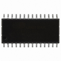
CS8420-CSZ Cirrus Logic Inc, CS8420-CSZ Datasheet - Page 28

CS8420-CSZ
Manufacturer Part Number
CS8420-CSZ
Description
IC SAMPLE RATE CONVERTER 28SOIC
Manufacturer
Cirrus Logic Inc
Type
Sample Rate Converterr
Specifications of CS8420-CSZ
Package / Case
28-SOIC
Applications
CD-R, DAT, DVD, MD, VTR
Mounting Type
Surface Mount
Operating Supply Voltage
5 V
Operating Temperature Range
- 10 C to + 70 C
Mounting Style
SMD/SMT
Resolution
17 bit to 24 bit
Control Interface
3 Wire, Serial
Supply Voltage Range
4.75V To 5.25V
Audio Ic Case Style
SOIC
No. Of Pins
28
Bandwidth
20kHz
Rohs Compliant
Yes
Audio Control Type
Volume
Dc
0841
Lead Free Status / RoHS Status
Lead free / RoHS Compliant
For Use With
598-1782 - EVALUATION BOARD FOR CS8420
Lead Free Status / Rohs Status
Lead free / RoHS Compliant
Other names
598-1125-5
Available stocks
Company
Part Number
Manufacturer
Quantity
Price
Company:
Part Number:
CS8420-CSZ
Manufacturer:
CIRRUS
Quantity:
319
Company:
Part Number:
CS8420-CSZ
Manufacturer:
CIRRUS
Quantity:
9 908
Part Number:
CS8420-CSZ
Manufacturer:
CIRRUS
Quantity:
20 000
Company:
Part Number:
CS8420-CSZ/D1
Manufacturer:
CIRRUS
Quantity:
378
Company:
Part Number:
CS8420-CSZR
Manufacturer:
NICHICON
Quantity:
4 200
28
8.
8.1
AES3 TRANSMITTER AND RECEIVER
Sample Rate Converter
The equation for the group delay through the sample rate converter, with the serial ports in Master mode is:
((input interface delay + 43) / F
The unit of delay depends on the frame rate (sample rate) F
frames. The AES transmitter, the serial input port, and the serial output port each have an interface delay
of 1 frame. The ± 0.5 frame delay in the second half of the equation is due to the start-up uncertainty of the
logic within the part.
When using multiple parts together, it is possible to start the parts simultaneously in a fashion that minimizes
the relative group delay between the parts. When multiple parts are started together in the proper way, the
variation in signal delay through the parts is ±1.5 μs.
To start the parts simultaneously, set up each one so that the PLL will lock, with the active input port driving
both output ports. Then simultaneously enable the RUN bits in all of the parts. TCBL on one of the CS8420
parts should be set as an output, while the remaining TCBL pins should be set as inputs. This synchronizes
the AES transmitter on all of the parts.
Depending upon software considerations, it may be advantageous to configure the registers so that an in-
terrupt is generated on the INT pin when lock occurs. The control logic should either poll the unlock bits until
all PLL’s are locked or wait for the interrupts to indicate that all are locked, depending on which approach
you’ve chosen.
When all of the PLL’s are locked, the CS8420’s should be advanced to the next state together. Drive all the
serial control ports together with the same clock and data. Change the configuration in register 03h accord-
ing to
Table 1
Table 1. Minimizing Group Delay Through Multiple CS8420s When Locking to RXP/RXN
Table 2. Minimizing Group Delay Through Multiple CS8420s When Locking to ILRCK
or
Register
Register
(HEX)
(HEX)
Table
01
03
04
01
03
04
11
11
2.
Initial Value
Initial Value
si
01 or 00
01 or 00
(HEX)
(HEX)
) + ((43 + output interface delay ± 0.5) / F
8A
95
41
10
40
10
State, After the PLL’s are Locked (HEX)
State, After the PLL’s are Locked (HEX)
Value After Advancing to the Running
Value After Advancing to the Running
s
. The AES receiver has a interface delay of 2
01 or 00
01 or 00
81
41
10
80
40
10
so
)
CS8420
DS245F4


