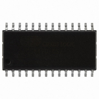
CS8420-CSZ Cirrus Logic Inc, CS8420-CSZ Datasheet - Page 81

CS8420-CSZ
Manufacturer Part Number
CS8420-CSZ
Description
IC SAMPLE RATE CONVERTER 28SOIC
Manufacturer
Cirrus Logic Inc
Type
Sample Rate Converterr
Specifications of CS8420-CSZ
Package / Case
28-SOIC
Applications
CD-R, DAT, DVD, MD, VTR
Mounting Type
Surface Mount
Operating Supply Voltage
5 V
Operating Temperature Range
- 10 C to + 70 C
Mounting Style
SMD/SMT
Resolution
17 bit to 24 bit
Control Interface
3 Wire, Serial
Supply Voltage Range
4.75V To 5.25V
Audio Ic Case Style
SOIC
No. Of Pins
28
Bandwidth
20kHz
Rohs Compliant
Yes
Audio Control Type
Volume
Dc
0841
Lead Free Status / RoHS Status
Lead free / RoHS Compliant
For Use With
598-1782 - EVALUATION BOARD FOR CS8420
Lead Free Status / Rohs Status
Lead free / RoHS Compliant
Other names
598-1125-5
Available stocks
Company
Part Number
Manufacturer
Quantity
Price
Company:
Part Number:
CS8420-CSZ
Manufacturer:
CIRRUS
Quantity:
319
Company:
Part Number:
CS8420-CSZ
Manufacturer:
CIRRUS
Quantity:
9 908
Part Number:
CS8420-CSZ
Manufacturer:
CIRRUS
Quantity:
20 000
Company:
Part Number:
CS8420-CSZ/D1
Manufacturer:
CIRRUS
Quantity:
378
Company:
Part Number:
CS8420-CSZR
Manufacturer:
NICHICON
Quantity:
4 200
DS245F4
15. CHANNEL STATUS AND USER DATA BUFFER MANAGEMENT
The CS8420 has a comprehensive channel status (C) and user (U) data buffering scheme, which allows automatic
management of channel status blocks and user data. Alternatively, sufficient control and access is provided to allow
the user to completely manage the C and U data via the control port.
15.1
AES3 Channel Status(C) Bit Management
The CS8420 contains sufficient RAM to store a full block of C data for both A and B channels (192x2 = 384
bits), and also 384 bits of U information. The user may read from or write to these RAMs via the control port.
Unlike the audio data, it is not possible to 'sample-rate' convert the C bits. This is because specific meanings
are associated with fixed-length data patterns, which should not be altered. Since the output data rate of the
CS8420 will differ from the input rate when sample-rate conversion is done, it is not feasible to directly trans-
fer incoming C data to the output. The CS8420 manages the flow of channel status data at the block level,
meaning that entire blocks of channel status information are buffered at the input, synchronized to the output
timebase, and then transmitted. The buffering scheme involves a cascade of three block-sized buffers,
named D,E, and F as shown in
stream. For example, the MSB of byte 0 (which is at control port address 20h) is the consumer/professional
bit for channel status block A.
The first buffer, D, accepts incoming C data from the AES receiver. The 2nd buffer, E, accepts entire blocks
of data from the D buffer. The E buffer is also accessible from the control port, allowing read and writing of
the C data. The 3rd buffer (F) is used as the source of C data for the AES3 transmitter. The F buffer accepts
block transfers from the E buffer.
If the input rate is slower than the output rate (so that in a given time interval, more channel status blocks
are transmitted than received), some buffered C blocks will be transmitted multiple times. If the input rate is
faster than the output rate, some will not be transmitted at all. This is illustrated in
channel status block integrity is maintained. If the transmitted sample count bits are important in the appli-
cation, then they will need to be updated via the control port by the microcontroller for every outgoing block.
From
AES3
Receiver
Figure 37. Channel Status Data Buffer Structure
Received
Data
Buffer
D
Figure
37. The MSB of each byte represents the first bit in the serial C data
8-bits
A
Control Port
words
E
8-bits
24
B
Transmit
Data
Buffer
F
To
AES3
Transmitter
(Figure
38). In this manner,
CS8420
81


