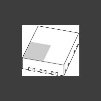
PMFPB6532UP NXP Semiconductors, PMFPB6532UP Datasheet - Page 5

PMFPB6532UP
Manufacturer Part Number
PMFPB6532UP
Description
Small-signal P-channel enhancement mode Field-Effect Transistor (FET) using Trench MOSFET technology and ultra low VF Maximum Efficiency General Application (MEGA) Schottky diode combined in a small and leadless ultra thin SOT1118 Surface-Mounted Dev
Manufacturer
NXP Semiconductors
Datasheet
1.PMFPB6532UP.pdf
(19 pages)
NXP Semiconductors
6. Thermal characteristics
PMFPB6532UP
Product data sheet
Fig 4.
Z
(K/W)
th(j-a)
10
10
10
1
3
2
10
FR4 PCB, standard footprint
duration; typical values
MOSFET transistor: Transient thermal impedance from junction to ambient as a function of pulse
−3
duty cycle = 1
0.25
0.5
0.1
0
0.75
0.33
0.05
0.02
0.01
0.2
Table 6.
[1]
[2]
Symbol
MOSFET transistor
R
R
Schottky diode
R
R
10
th(j-a)
th(j-sp)
th(j-a)
th(j-sp)
−2
Device mounted on an FR4 PCB, single-sided copper, tin-plated and standard footprint.
Device mounted on an FR4 PCB, single-sided copper, tin-plated, mounting pad for drain 6 cm
Thermal characteristics
Parameter
thermal resistance from
junction to ambient
thermal resistance from
junction to solder point
thermal resistance from
junction to ambient
thermal resistance from
junction to solder point
All information provided in this document is subject to legal disclaimers.
10
−1
20 V, 3.5 A / 320 mV V
Rev. 1 — 9 March 2011
1
Conditions
in free air
in free air
F
P-channel MOSFET-Schottky combination
10
PMFPB6532UP
[1]
[2]
[1]
[2]
Min
-
-
-
-
-
-
10
2
Typ
-
-
-
-
-
-
t
p
© NXP B.V. 2011. All rights reserved.
(s)
017aaa067
Max
240
100
15
260
105
15
10
2
.
3
Unit
K/W
K/W
K/W
K/W
K/W
K/W
5 of 19


