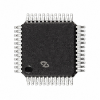
LM98501CCVBH National Semiconductor, LM98501CCVBH Datasheet

LM98501CCVBH
Specifications of LM98501CCVBH
Related parts for LM98501CCVBH
LM98501CCVBH Summary of contents
Page 1
... Video conferencing n Security camera n Plain paper copier n Flatbed or handheld color scanner n Video processing for x-ray or infrared n Barcode scanner Typical Digital Camera Block Diagram © 2000 National Semiconductor Corporation Features n +3V single power supply n Low power CMOS design n 4-wire serial interface enables pixel-rate n 2 ...
Page 2
... Overall Chip Block Diagram LM98501 Chip Pin Out Ordering Information LM98501CCVBH www.national.com FIGURE 1. Chip Block Diagram FIGURE 2. Pin Out Diagram Commercial NS Package (0˚C T +70˚C) A LQFP 2 DS101292-2 DS101292-3 ...
Page 3
Typical Application Circuit Pin Descriptions Pin Name I/O Typ 1 AUX AGND AGND ACLP RESET AV ...
Page 4
Pin Descriptions (Continued) Pin Name I/O Typ 11 DV CLK SHP SHD BOL BLKCLP REFP REFN ...
Page 5
Pin Descriptions (Continued) Pin Name I/O Typ 46 AOUT AV AGND P Legend Input Output), (IO = Bi-directional Power Digital Analog). Description Positive differential analog ...
Page 6
... Absolute Maximum Ratings If Military/Aerospace specified devices are required, please contact the National Semiconductor Sales Office/ Distributors for availability and specifications. Any Positive Supply Voltage Voltage on Any Input or Output Pin Input Current at Any Pin (Note 3) Package Input Current (Note 3) = 25˚C Package Dissipation at T ...
Page 7
Correlated Double Sampler Specifications The following specifications apply for DV I/O = +3.0V, C noted. Boldface limits apply for T A Symbol Parameter V Input Voltage Level IN I Input Leakage Current IN C Input ...
Page 8
AC Electrical Characteristics The following specifications apply for DV I/O = +3.0V Boldface limits apply for T A MIN Symbol Parameter f Input Clock Frequency CLK T Input Clock Period CLK t ...
Page 9
Typical Performance Characteristics DNL vs. Temperature DNL vs. Clock Frequency INL vs. Temperature DNL vs. Supply Voltage DS101292-19 DNL vs. Clock Duty Supply DS101292-21 INL vs. Supply Voltage DS101292-23 9 DS101292-20 DS101292-22 DS101292-24 www.national.com ...
Page 10
Typical Performance Characteristics INL vs. Clock Frequency Power Dissipation vs. Temperature Actual vs. Ideal PGA Gain and Clock Frequency www.national.com (Continued) INL vs. Clock Duty Cycle DS101292-25 Power Dissipation vs. Clock Frequency DS101292-27 PGA Gain vs. Supply Voltage and Clock ...
Page 11
Typical Performance Characteristics @ Grounded Input Noise 20 MHz Clock Frequency Spectral Response @ 20 MHz Clock Frequency DNL vs. Power Setting @ 27 MHz Clock Frequency (Continued) Grounded Input Noise DS101292-31 Spectral Response DS101292-33 Power Dissipation vs. Power Setting ...
Page 12
CDS Sampling Timing 1 SHP overrides the CLAMP signal’s falling edge for sampling the reset voltage (SHP is active-low by default). 2 The CLAMP signal is an internal signal derived from the CLK input whose falling edge samples the CCD ...
Page 13
Digital Output Timing System Timing System Overview INTRODUCTION The LM98501 is a 10-bit, complete analog-to-digital camera signal processor for use with CCD imager systems operating from a single +3V supply. The internal processing is carefully optimized to maintain the signal-to-noise ...
Page 14
System Overview (Continued) FIGURE 9. Correlated Double Sampling PROGRAMMABLE GAIN AMPLIFIER In a CCD imager, there may be millions of photo diodes that normally have some gain variation from pixel to pixel. Other gain errors are generated by the amount ...
Page 15
System Overview (Continued) ANALOG CLAMP During optical black pixels, an offset often appears on the CCD generated input signal. This offset may be seen by the CDS circuitry as a valid video signal rather than the actual black level signal; ...
Page 16
System Overview (Continued) FIGURE 11. ADC Output vs. Black Level Register Value COLOR FILTER ARRAY (CFA) CONFIGURATION In order to utilize the LM98501’s programmable pixel-rate gain, a color filter array (CFA) pattern must be defined. Some commonly used CFA patterns ...
Page 17
Register Memory Map PGA Gain 0 PGA Gain 1 PGA Gain 2 PGA Gain 3 Analog Offset 0 Analog Offset 1 Analog Offset 2 Analog Offset 3 CFA Configuration 0 CFA Configuration 1 CFA Definition Output Black Level Software Control ...
Page 18
Register Data (Continued) Bit Bit Symbol [7:0] Signed Analog Digital representation of the Offset analog offset to be applied to the input of the PGA. See “Analog Offset” on page 15. Register Name Analog Offset 3 Address 7 Hex Type ...
Page 19
Register Data (Continued) Bit Bit Symbol Description [3] Offset Enables the digital black Auto-Calibration level correction loop. Analog Enable offset registers are read-only when offset auto-calibration is enabled. [2] SHP/SHD Inverts the SHP and SHD Active-HIGH inputs causing the CDS ...
Page 20
Serial Interface Timing Specifications The following specifications apply AV I/O = +3.0V Boldface limits apply for T A MIN Symbol Parameter t SCLK Period MIN SCLK Duty Cycle SCLK Rise/Fall Time t ...
Page 21
PGA Gain Plots FIGURE 15. PGA Gain (Linear Scale) vs. PGA Gain Code FIGURE 16. PGA Gain (Logarithmic Scale) vs. PGA Gain Code Applications Information ANALOG-TO-DIGITAL CONVERTER REFERENCE BYPASSING Figure 17 shows a simple reference bypassing scheme with minimal components. ...
Page 22
Applications Information ANALOG OFFSET DAC RANGE ADJUSTMENT The analog offset DAC has an input range of Register Data ). This analog offset corresponds to approxi- mately 0.4 LSB at the ADC output per DAC input code LSB step. Therefore, the ...
Page 23
Applications Information (Continued) FIGURE 18. Recommended Layout Pattern 23 DS101292-17 www.national.com ...
Page 24
... National does not assume any responsibility for use of any circuitry described, no circuit patent licenses are implied and National reserves the right at any time without notice to change said circuitry and specifications. inches (millimeters) unless otherwise noted 48-Lead LQFP Package Order Number LM98501CCVBH NS Package Number VBH48A 2. A critical component is any component of a life ...


