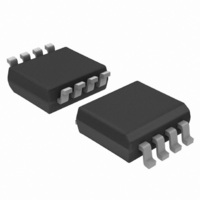
74LVC1G74DC,125 NXP Semiconductors, 74LVC1G74DC,125 Datasheet - Page 6

74LVC1G74DC,125
Manufacturer Part Number
74LVC1G74DC,125
Description
IC SNGL D FF POS-EDG TRIG 8VSSOP
Manufacturer
NXP Semiconductors
Series
74LVCr
Type
D-Typer
Datasheet
1.74LVC1G74DC125.pdf
(25 pages)
Specifications of 74LVC1G74DC,125
Output Type
Differential
Package / Case
US8, 8-VSSOP
Function
Set(Preset) and Reset
Number Of Elements
1
Number Of Bits Per Element
1
Frequency - Clock
200MHz
Trigger Type
Positive Edge
Current - Output High, Low
32mA, 32mA
Voltage - Supply
1.65 V ~ 5.5 V
Operating Temperature
-40°C ~ 125°C
Mounting Type
Surface Mount
Number Of Circuits
1
Logic Family
74LVC
Logic Type
CMOS
Polarity
Inverting/Non-Inverting
Input Type
Single-Ended
Propagation Delay Time
13.4 ns
High Level Output Current
- 32 mA
Low Level Output Current
32 mA
Supply Voltage (max)
5.5 V
Maximum Operating Temperature
+ 125 C
Mounting Style
SMD/SMT
Minimum Operating Temperature
- 40 C
Supply Voltage (min)
1.65 V
Technology
CMOS
Number Of Bits
1
Number Of Elements
1
Clock-edge Trigger Type
Positive-Edge
Operating Supply Voltage (typ)
1.8/2.5/3.3/5V
Package Type
VSSOP
Operating Supply Voltage (min)
1.65V
Operating Supply Voltage (max)
5.5V
Operating Temp Range
-40C to 125C
Operating Temperature Classification
Automotive
Mounting
Surface Mount
Pin Count
8
Lead Free Status / RoHS Status
Lead free / RoHS Compliant
Delay Time - Propagation
-
Lead Free Status / Rohs Status
Lead free / RoHS Compliant
Other names
568-4494-2
74LVC1G74DC-G
74LVC1G74DC-G
935274973125
74LVC1G74DC-G
74LVC1G74DC-G
935274973125
NXP Semiconductors
8. Limiting values
Table 6.
In accordance with the Absolute Maximum Rating System (IEC 60134). Voltages are referenced to GND (ground = 0 V).
[1]
[2]
[3]
9. Recommended operating conditions
Table 7.
74LVC1G74
Product data sheet
Symbol
V
I
V
I
V
I
I
I
P
T
Symbol
V
V
V
T
Δt/ΔV
IK
OK
O
CC
GND
stg
amb
CC
I
O
tot
CC
I
O
The input and output voltage ratings may be exceeded if the input and output current ratings are observed.
When V
For TSSOP8 packages: above 55 °C the value of P
For VSSOP8 packages: above 110 °C the value of P
For XSON8, XSON8U and XQFN8U packages: above 118 °C the value of P
CC
Limiting values
Operating conditions
Parameter
supply voltage
input voltage
output voltage
ambient temperature
input transition rise and fall rate
= 0 V (Power-down mode), the output voltage can be 5.5 V in normal operation.
Parameter
supply voltage
input clamping current
input voltage
output clamping current
output voltage
output current
supply current
ground current
total power dissipation
storage temperature
All information provided in this document is subject to legal disclaimers.
Conditions
V
V
Active mode
Power-down mode
V
T
amb
I
O
O
< 0 V
> V
= 0 V to V
tot
Single D-type flip-flop with set and reset; positive edge trigger
Rev. 9 — 5 August 2010
tot
= −40 °C to +125 °C
Conditions
Active mode
Power-down mode; V
V
V
derates linearly with 2.5 mW/K.
CC
derates linearly with 8.0 mW/K.
CC
CC
or V
= 1.65 V to 2.7 V
= 2.7 V to 5.5 V
CC
O
< 0 V
tot
CC
derates linearly with 7.8 mW/K.
= 0 V
[1][2]
[1]
[1]
[3]
Min
−0.5
−50
−0.5
-
−0.5
−0.5
-
-
−100
-
−65
0
0
Min
1.65
0
−40
-
-
74LVC1G74
Max
+6.5
-
+6.5
±50
V
+6.5
±50
100
-
300
+150
CC
© NXP B.V. 2010. All rights reserved.
+ 0.5
Max
5.5
5.5
V
5.5
+125
20
10
CC
Unit
V
mA
V
mA
V
V
mA
mA
mA
mW
°C
V
Unit
V
V
V
°C
ns/V
ns/V
6 of 25


