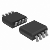
74LVC1G74DC,125 NXP Semiconductors, 74LVC1G74DC,125 Datasheet - Page 9

74LVC1G74DC,125
Manufacturer Part Number
74LVC1G74DC,125
Description
IC SNGL D FF POS-EDG TRIG 8VSSOP
Manufacturer
NXP Semiconductors
Series
74LVCr
Type
D-Typer
Datasheet
1.74LVC1G74DC125.pdf
(25 pages)
Specifications of 74LVC1G74DC,125
Output Type
Differential
Package / Case
US8, 8-VSSOP
Function
Set(Preset) and Reset
Number Of Elements
1
Number Of Bits Per Element
1
Frequency - Clock
200MHz
Trigger Type
Positive Edge
Current - Output High, Low
32mA, 32mA
Voltage - Supply
1.65 V ~ 5.5 V
Operating Temperature
-40°C ~ 125°C
Mounting Type
Surface Mount
Number Of Circuits
1
Logic Family
74LVC
Logic Type
CMOS
Polarity
Inverting/Non-Inverting
Input Type
Single-Ended
Propagation Delay Time
13.4 ns
High Level Output Current
- 32 mA
Low Level Output Current
32 mA
Supply Voltage (max)
5.5 V
Maximum Operating Temperature
+ 125 C
Mounting Style
SMD/SMT
Minimum Operating Temperature
- 40 C
Supply Voltage (min)
1.65 V
Technology
CMOS
Number Of Bits
1
Number Of Elements
1
Clock-edge Trigger Type
Positive-Edge
Operating Supply Voltage (typ)
1.8/2.5/3.3/5V
Package Type
VSSOP
Operating Supply Voltage (min)
1.65V
Operating Supply Voltage (max)
5.5V
Operating Temp Range
-40C to 125C
Operating Temperature Classification
Automotive
Mounting
Surface Mount
Pin Count
8
Lead Free Status / RoHS Status
Lead free / RoHS Compliant
Delay Time - Propagation
-
Lead Free Status / Rohs Status
Lead free / RoHS Compliant
Other names
568-4494-2
74LVC1G74DC-G
74LVC1G74DC-G
935274973125
74LVC1G74DC-G
74LVC1G74DC-G
935274973125
NXP Semiconductors
11. Dynamic characteristics
Table 9.
Voltages are referenced to GND (ground = 0 V); for test circuit see
74LVC1G74
Product data sheet
Symbol Parameter
t
t
pd
W
propagation delay CP to Q, Q; see
pulse width
Dynamic characteristics
Conditions
SD to Q, Q; see
RD to Q, Q; see
CP HIGH or LOW;
see
SD and RD LOW;
see
V
V
V
V
V
V
V
V
V
V
V
V
V
V
V
V
V
V
V
V
V
V
V
V
V
CC
CC
CC
CC
CC
CC
CC
CC
CC
CC
CC
CC
CC
CC
CC
CC
CC
CC
CC
CC
CC
CC
CC
CC
CC
Figure 8
Figure 9
= 1.65 V to 1.95 V
= 2.3 V to 2.7 V
= 2.7 V
= 3.0 V to 3.6 V
= 4.5 V to 5.5 V
= 1.65 V to 1.95 V
= 2.3 V to 2.7 V
= 2.7 V
= 3.0 V to 3.6 V
= 4.5 V to 5.5 V
= 1.65 V to 1.95 V
= 2.3 V to 2.7 V
= 2.7 V
= 3.0 V to 3.6 V
= 4.5 V to 5.5 V
= 1.65 V to 1.95 V
= 2.3 V to 2.7 V
= 2.7 V
= 3.0 V to 3.6 V
= 4.5 V to 5.5 V
= 1.65 V to 1.95 V
= 2.3 V to 2.7 V
= 2.7 V
= 3.0 V to 3.6 V
= 4.5 V to 5.5 V
All information provided in this document is subject to legal disclaimers.
Figure 8
Figure 9
Figure 9
Single D-type flip-flop with set and reset; positive edge trigger
Rev. 9 — 5 August 2010
[2]
[2]
[2]
Figure
Min
1.5
1.0
1.0
1.0
1.0
1.5
1.0
1.0
1.0
1.0
1.5
1.0
1.0
1.0
1.0
6.2
2.7
2.7
2.7
2.0
6.2
2.7
2.7
2.7
2.0
−40 °C to +85 °C
10.
Typ
6.0
3.5
3.5
3.5
2.5
6.0
3.5
3.5
3.0
2.5
5.0
3.5
3.5
3.0
2.5
1.3
1.6
-
-
-
-
-
-
-
-
[1]
Max
13.4
12.9
12.9
7.1
7.1
5.9
4.1
7.0
7.0
5.9
4.1
7.0
7.0
5.9
4.1
-
-
-
-
-
-
-
-
-
-
−40 °C to +125 °C
Min
1.5
1.0
1.0
1.0
1.0
1.5
1.0
1.0
1.0
1.0
1.5
1.0
1.0
1.0
1.0
6.2
2.7
2.7
2.7
2.0
6.2
2.7
2.7
2.7
2.0
74LVC1G74
© NXP B.V. 2010. All rights reserved.
Max
13.4
12.9
12.9
7.1
7.1
5.9
4.1
7.0
7.0
5.9
4.1
7.0
7.0
5.9
4.1
-
-
-
-
-
-
-
-
-
-
Unit
ns
ns
ns
ns
ns
ns
ns
ns
ns
ns
ns
ns
ns
ns
ns
ns
ns
ns
ns
ns
ns
ns
ns
ns
ns
9 of 25


